One-transistor dynamic random access memory (DRAM) unit based on silicon-germanium silicon heterojunction, and method for preparing one-transistor DRAM unit

A single-transistor, heterojunction technology, applied in the direction of transistors, semiconductor/solid-state device manufacturing, electrical components, etc., can solve the problems of small difference, unfavorable DRAM working stability, high working voltage of transistors, etc.

Inactive Publication Date: 2012-05-02
SHANGHAI HUALI MICROELECTRONICS CORP
View PDF6 Cites 4 Cited by
  • Summary
  • Abstract
  • Description
  • Claims
  • Application Information

AI Technical Summary

Problems solved by technology

[0006] Therefore, the existing 1T-DRAM still has the following defects: for example, the operating voltage of the transistor is too high, and the difference between the source an

Method used


Image

  • One-transistor dynamic random access memory (DRAM) unit based on silicon-germanium silicon heterojunction, and method for preparing one-transistor DRAM unit
  • One-transistor dynamic random access memory (DRAM) unit based on silicon-germanium silicon heterojunction, and method for preparing one-transistor DRAM unit
  • One-transistor dynamic random access memory (DRAM) unit based on silicon-germanium silicon heterojunction, and method for preparing one-transistor DRAM unit

Examples


Embodiment Construction

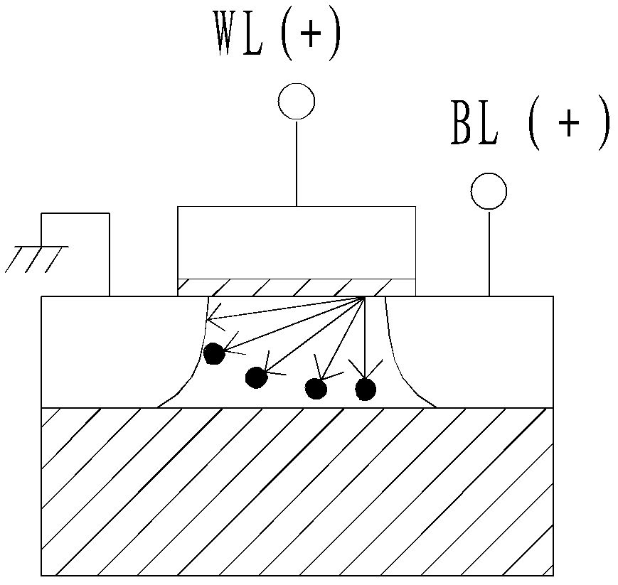
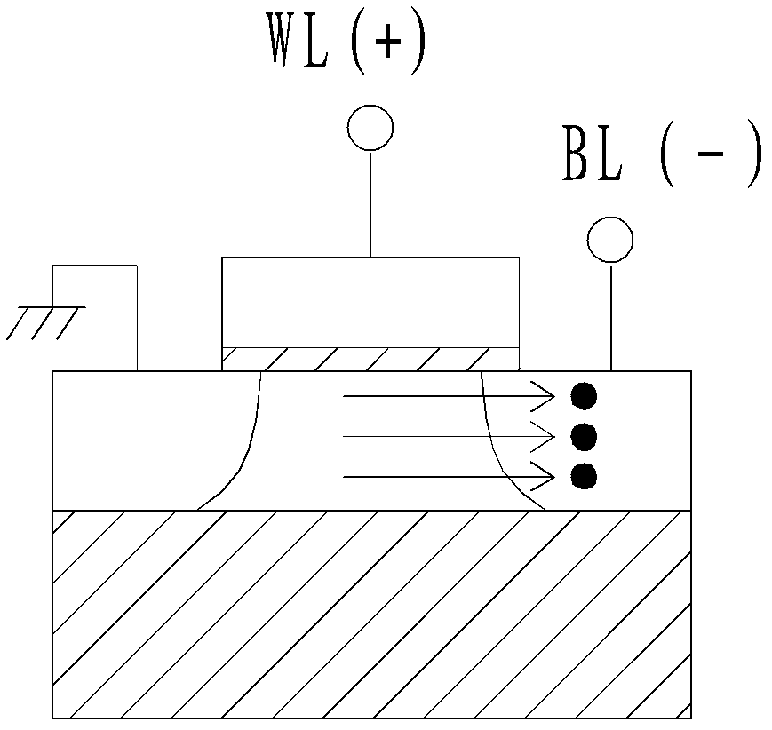
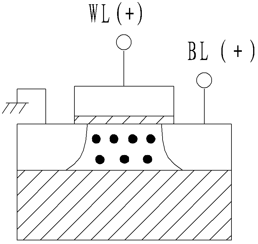
[0024] 1T-DRAM is generally a SOI (silicon on insulator) floating body (floating body) transistor. When charging its body region, it completes the write "1" operation through the accumulation of holes in the body region. At this time, due to the hole in the body region Accumulated to cause the substrate effect, resulting in a decrease in the threshold voltage of the transistor. When the body region is discharged, the hole accumulated in the body region is discharged through the body drain or the body-source PN junction forward bias (forward bias) to complete the write "0" operation, and the substrate effect disappears at this time. The threshold voltage returns to normal. The turn-on current increases. The read operation is to read the source-leakage current when the transistor is on. Since the threshold voltages of the "1" and "0" states are different, the source-leakage currents of the two are also different. When the source-leakage current is large, it means read When the...


PUM


Abstract

The invention discloses a one-transistor dynamic random access memory (DRAM) unit based on a silicon-germanium silicon heterojunction and a method for preparing the one-transistor DRAM unit. The method for preparing the single-transistor DRAM unit comprises the following steps of: forming a SiGe epitaxial layer in the top layer of a silicon wafer on an insulator; performing a surface dry oxidization process on the SiGe epitaxial layer so as to form a first conductive type SiGe body region, wherein the dry oxidization process is not stopped until a valence band position of the first conductive type SiGe body region is higher than that of the material of the top layer of the silicon wafer on the insulator according to a mole ratio of the germanium content in the first conductive type SiGe body region; and forming an N-channel metal oxide semiconductor (NMOS) transistor comprising the heterojunction based on silicon-germanium silicon in the silicon wafer on the insulator, wherein the NMOS transistor is a single transistor. The 1T-DRAM unit can effectively reduce the working voltage and increase the balance of output current between readings '0' and '1', namely the signal margin is increased.

Description

technical field [0001] The present invention generally relates to a method for preparing a capacitive (Capacitorless) dynamic random access memory (DRAM), in particular to a single-transistor dynamic random access memory (1T-DRAM) cell structure based on a silicon-germanium-silicon heterojunction and its preparation method. Background technique [0002] As the feature size of semiconductor integrated circuit devices continues to shrink, for traditional single transistor / single capacitor (1T / 1C) embedded (embedded) DRAM cells, the capacitance generally includes stack capacitors or deep trenches. deep-trench capacitor, etc., in order to obtain sufficient storage capacity (generally requires 30fF / unit), the capacitance manufacturing process of the DRAM unit will become more and more complicated, and the compatibility with the logic device process will become more and more Difference. Therefore, a capless DRAM with good compatibility with logic devices will have a good develop...

Claims


Application Information

Patent Timeline
IPC IPC(8): H01L21/8242H01L29/06H01L27/108
Inventor 黄晓橹陈玉文
Owner SHANGHAI HUALI MICROELECTRONICS CORP
Why Eureka
Try Eureka