Silicon carbide bipolar transistor based on active region trench structure and manufacturing method thereof

A bipolar transistor and active region technology, applied in the field of microelectronics, can solve problems such as low breakdown voltage, achieve the effects of improved breakdown voltage, compatible manufacturing process, improved base transfer efficiency and current gain

Active Publication Date: 2017-05-17
XIDIAN UNIV
View PDF4 Cites 4 Cited by
  • Summary
  • Abstract
  • Description
  • Claims
  • Application Information

AI Technical Summary

Problems solved by technology

[0005] In summary, the existing SiC bipolar transistors have a thin base structure that may lead to a low breakdown voltage

Method used


Image

  • Silicon carbide bipolar transistor based on active region trench structure and manufacturing method thereof
  • Silicon carbide bipolar transistor based on active region trench structure and manufacturing method thereof
  • Silicon carbide bipolar transistor based on active region trench structure and manufacturing method thereof

Examples


Embodiment 1

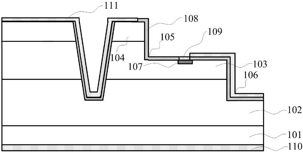
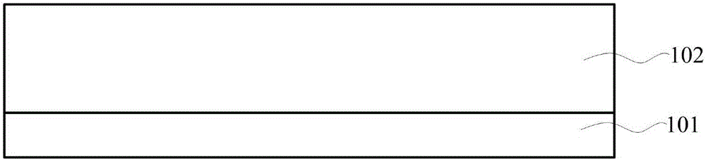
[0043] In the first step, the N − collector region 102 is epitaxially grown on the N+ substrate 101 . Specifically, such as Figure 2A As shown, the N+ substrate 101 is firstly cleaned by RCA standard; and then the front surface of the N+ substrate 101 is epitaxially grown with a thickness of 6 μm and a nitrogen ion doping concentration of 3×10 15 cm-3 N-collector region 102 .

[0044] It should be noted that the growth conditions of the N-collector region 102 are: the epitaxial process conditions are: temperature 1600°C, pressure 100mbar, reaction gas is silane and propane, carrier gas is pure hydrogen, and impurity source is liquid nitrogen.

[0045] It should be noted that the RCA standard cleaning method was first created by Kern and Puotinen in the RCA laboratory of N.J.Princeton in 1965, and thus got its name. RCA is a typical wet chemical cleaning method that is still the most commonly used. The cleaning method mainly includes the following cleaning solutions.

[004...

Embodiment 2

[0071] In step 1, epitaxially grow the N− collector region 102 on the N+ substrate 101 . Specifically, such as Figure 2A As shown, the N+ substrate 101 is firstly cleaned by RCA standard; then, on the front of the N+ substrate 101, the epitaxial growth thickness is 6.5 μm, and the nitrogen ion doping concentration is 6×10 15 cm -3 N-collector region 102 .

[0072] It should be noted that the growth conditions of the N-collector region 102 are as follows: the temperature is 1600° C., the pressure is 100 mbar, the reaction gas is silane and propane, the carrier gas is pure hydrogen, and the impurity source is liquid nitrogen.

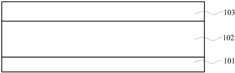
[0073] Step 2, growing the base region 103 epitaxially on the N − collector region 102 . Specifically, such as Figure 2B As shown, on the N- collector region 102, the epitaxial growth thickness is 0.7 μm and the doping concentration of aluminum ions is 1×10 17 cm -3 base region 103 .

[0074] It should be noted that the growth process conditions of...

Embodiment 3

[0093] In step A, epitaxially grow the N− collector region 102 on the N+ substrate 101 . Specifically, such as Figure 2A As shown, the N+ substrate 101 is firstly cleaned by RCA standard; then, the epitaxial growth thickness is 7 μm and the nitrogen ion doping concentration is 1×10 16 cm -3 N-collector region 102 .

[0094] It should be noted that the growth conditions of the N-collector region 102 are as follows: the temperature is 1600° C., the pressure is 100 mbar, the reaction gas is silane and propane, the carrier gas is pure hydrogen, and the impurity source is liquid nitrogen.

[0095] In step B, the base region 103 is epitaxially grown on the N − collector region 102 . Specifically, such as Figure 2B As shown, on the N- collector region 102, the epitaxial growth thickness is 0.8 μm and the doping concentration of aluminum ions is 5×10 17 cm -3 base region 103 .

[0096] It should be noted that the growth process conditions of the base region 103 are as follows...


PUM


Abstract

The invention discloses a silicon carbide bipolar transistor based on an active region trench structure. The invention belongs to the technical field of microelectronics. The mentioned transistor can solve the problem that a thin substrate structure of the existing silicon bipolar transistor may lead to low breakdown voltage. The transistor comprises N+ launching area that is provided on the surface of the base, a device groove that is in the form of incline groove, a launching zone platform with vertical groove type and a device isolation zone. Base P + an injection zone is placed on lower surface of the launching zone platform and in the base and the device groove is provided in the N+ the launching area and extended to the upper part of a N- collector area while the device isolation zone is provided in the base and extended to the upper part of the N- collector zone.

Description

technical field [0001] The invention belongs to the technical field of microelectronics, and relates to a semiconductor device, in particular to a silicon carbide bipolar transistor based on an active region trench structure and a manufacturing method thereof. Background technique [0002] With the rapid development of power electronics technology, the demand for high-power semiconductor devices is becoming more and more significant. Due to the limitation of materials, the characteristics of traditional silicon devices have reached its theoretical limit. Silicon carbide is a wide bandgap semiconductor material that has been developed rapidly in the past ten years. It has wide bandgap, high thermal conductivity, and high carrier saturation migration. High efficiency, high power density and other advantages, can be applied to high power, high temperature and radiation resistance and other application fields. Among them, the oxide layer-based MOSFET (English: Metal-Oxide-Semic...

Claims


Application Information

Patent Timeline
Patent Type & Authority Applications(China)
IPC IPC(8): H01L29/732H01L29/06H01L29/16H01L21/331
Inventor 元磊李钊君宋庆文汤晓燕张艺蒙张玉明
Owner XIDIAN UNIV
Why Eureka
Try Eureka