Techniques for providing decoupling capacitance

a capacitance decoupling and capacitance technology, applied in the field of electronic devices, can solve the problems of increasing the area of printed circuit boards required to interconnect, increasing the complexity of ceramic substrates, and reducing production yields

Inactive Publication Date: 2007-02-15
IBM CORP
View PDF11 Cites 61 Cited by
  • Summary
  • Abstract
  • Description
  • Claims
  • Application Information

AI Technical Summary

Benefits of technology

[0008] Electronic devices and techniques for the fabrication thereof are provided. In one aspect of the invention, an electronic device is provided. The electronic device comprises at least one interposer structure having one

Problems solved by technology

However, when a device requires a large number of IC chips, individually packaging and mounting each chip greatly increases the area on the printed circuit board required to interconnect all the chips.
Conventionally, decoupling capacitors have been incorporated into the ceramic substrate which increases the comp

Method used


Image

  • Techniques for providing decoupling capacitance
  • Techniques for providing decoupling capacitance
  • Techniques for providing decoupling capacitance

Examples


Embodiment Construction

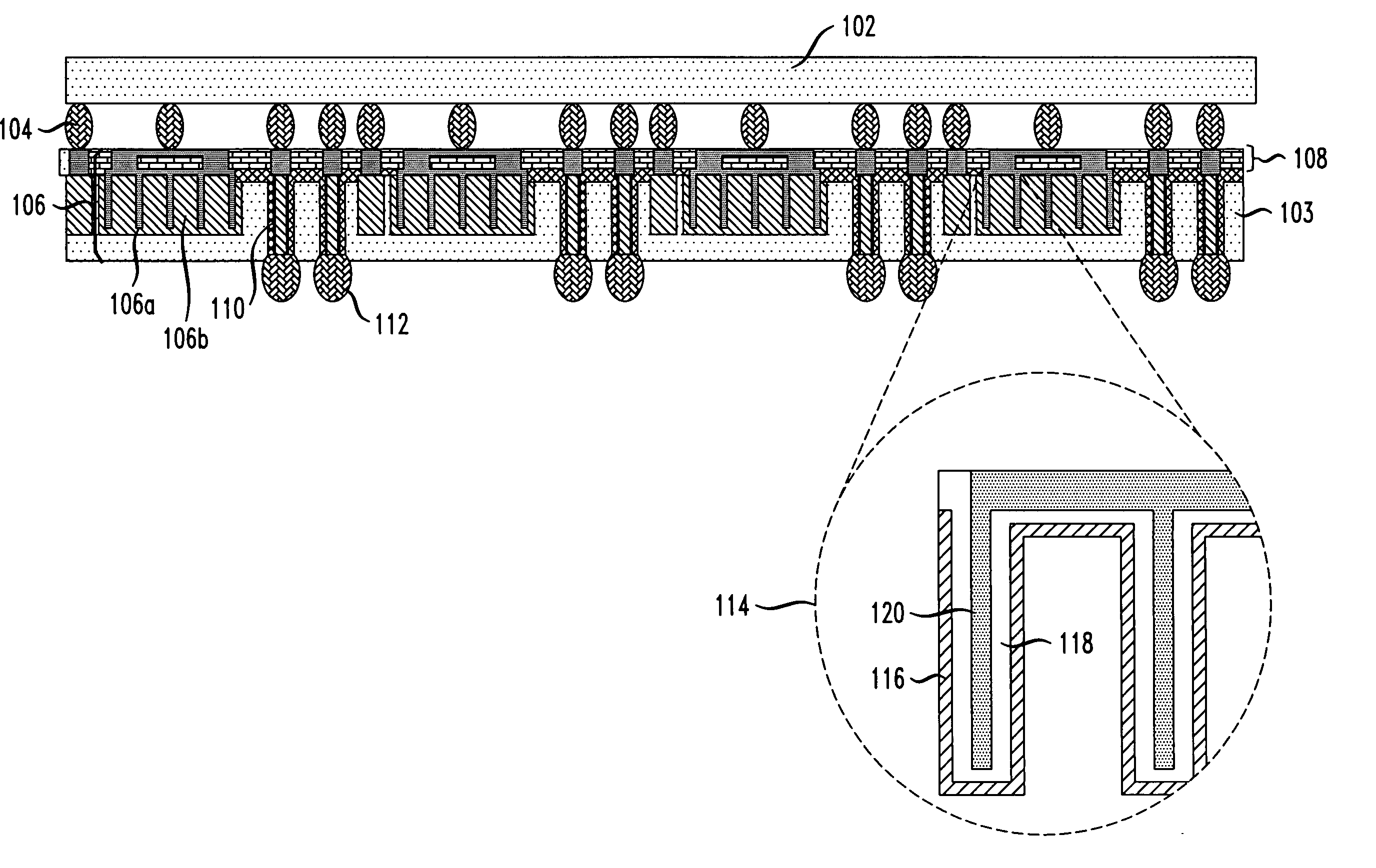
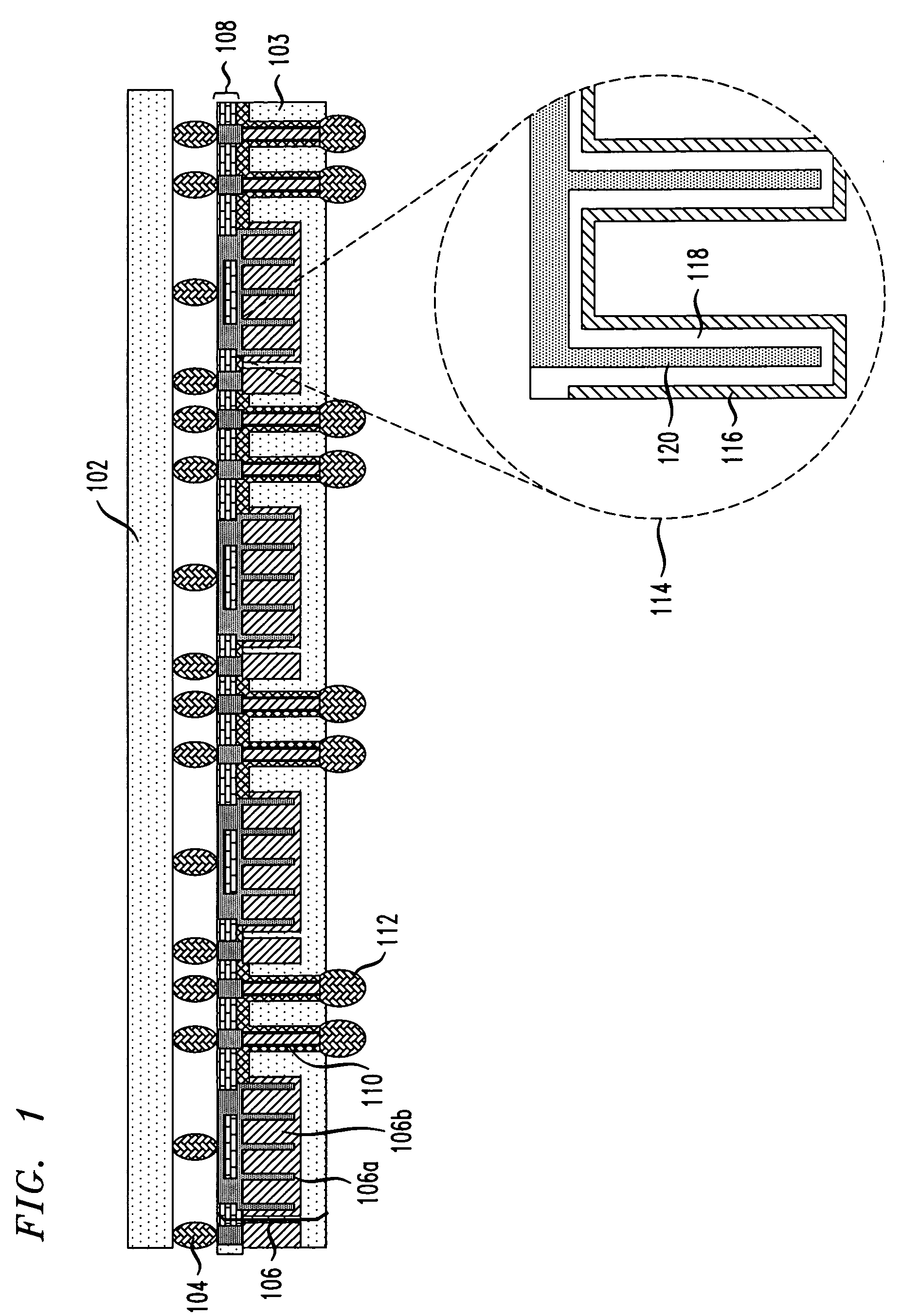
[0022]FIG. 1 is a diagram illustrating a cross-sectional view of exemplary electronic device 100 comprising an interposer structure having a plurality of capacitors integrated therein. Electronic device 100 comprises integrated circuit (IC) chip 102 and interposer structure 103 linked by a plurality of interconnections 104. Interconnections 104 may comprise any suitable electrically conductive material, including, but not limited to solder materials, such as lead-tin or tin-silver solder, copper, and combinations comprising at least one of the foregoing materials.

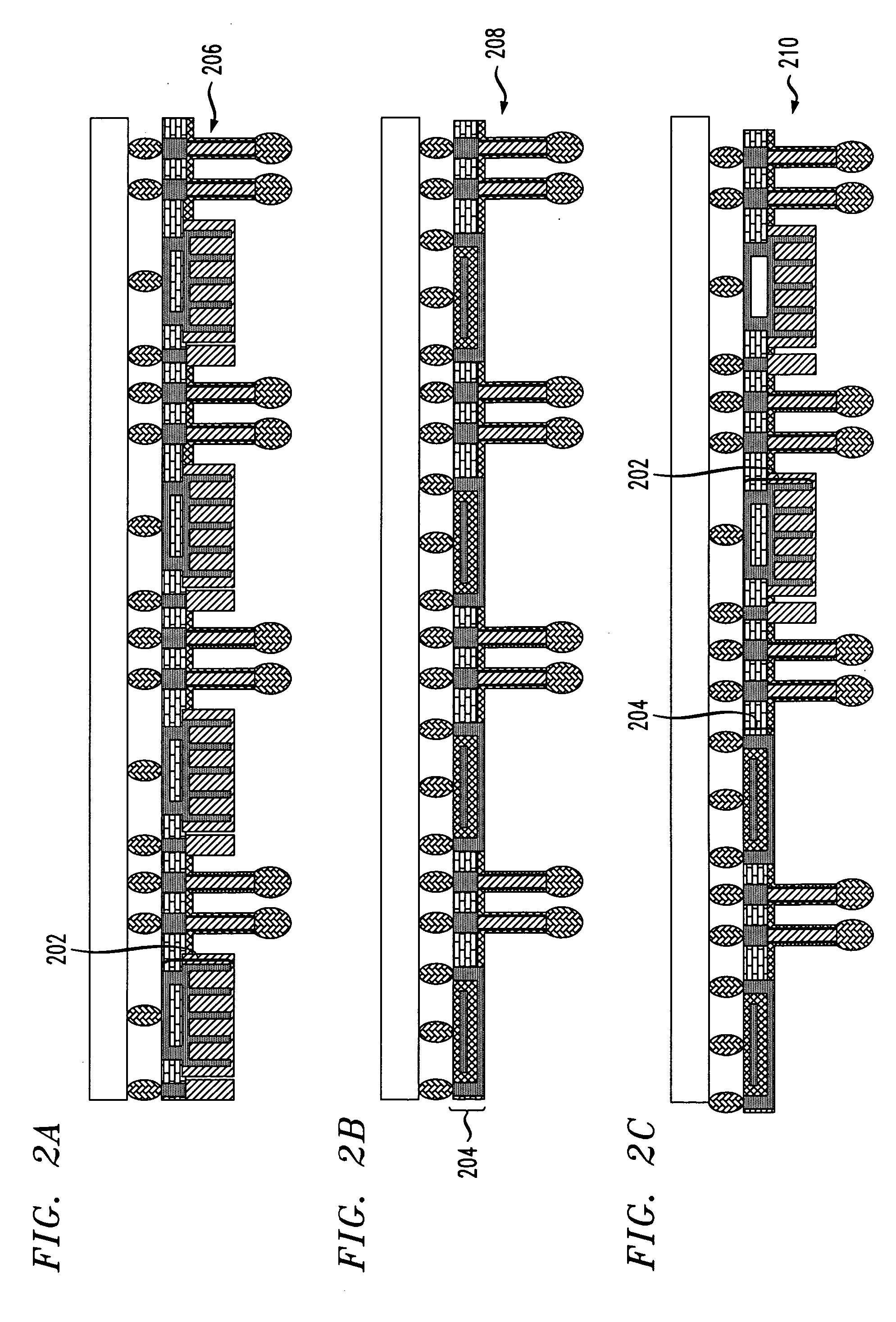
[0023] Interposer structure 103 comprises a plurality of decoupling capacitors 106 and vias 110. Decoupling capacitors 106, as shown in FIG. 1, comprise trench capacitors. However, as will be described in detail below, other suitable types of decoupling capacitors, such as parallel plate capacitors may used instead of, or in addition to, trench capacitors.

[0024] As shown, for example, in expanded view 114, a trench decoup...


PUM


Abstract

Techniques for electronic device fabrication are provided. In one aspect, an electronic device is provided. The electronic device comprises at least one interposer structure having one or more vias and a plurality of decoupling capacitors integrated therein, the at least one interposer structure being configured to allow for one or more of the plurality of decoupling capacitors to be selectively deactivated. In another aspect, a method of fabricating an electronic device comprising at least one interposer structure having one or more vias and a plurality of decoupling capacitors integrated therein comprises the following step. One or more of the plurality of decoupling capacitors are selectively deactivated.

Description

FIELD OF THE INVENTION [0001] The present invention relates to electronic devices and, more particularly, to techniques for providing decoupling capacitance in electronic devices. BACKGROUND OF THE INVENTION [0002] Many electronic devices use a number of separate integrated circuit (IC) chips. Typically, each IC chip is mounted individually in a separate package that is connected to a printed circuit board which provides power and signal interconnections to the IC chips. However, when a device requires a large number of IC chips, individually packaging and mounting each chip greatly increases the area on the printed circuit board required to interconnect all the chips. Additionally, as device speeds increase, it is more important to minimize the path lengths between IC chips themselves, as well as between the IC chips and other electronic components connected to them. [0003] To decrease printed circuit board space, distance between IC chips and complexity of interconnections, many d...

Claims


Application Information

Patent Timeline
IPC IPC(8): H01L23/48
CPCH01L23/49822H01L23/49827H01L23/50H01L23/5382H01L2924/01012H01L2224/16235H01L2924/01077H01L2924/01078H01L2924/15311H01L2224/16225H01L2924/01019H01L2924/0102
Inventor HORTON, RAYMOND R.KNICKERBOCKER, JOHN U.SPROGIS, EDMUND J.TSANG, CORNELIA K.
Owner IBM CORP
Why Eureka
Try Eureka