Switch element, memory element and magnetoresistive effect element

a technology of magnetoresistive effect and memory element, which is applied in the direction of magnetic field-controlled resistors, digital storage, instruments, etc., can solve the problems of not being suitable for mass production, not having a selective growth method of carbon nanotube having a specific structure, and significantly deteriorating element properties

Inactive Publication Date: 2007-02-15
KK TOSHIBA
View PDF7 Cites 39 Cited by
  • Summary
  • Abstract
  • Description
  • Claims
  • Application Information

AI Technical Summary

Benefits of technology

[0021] According to still another aspect of the present invention, a magnetoresistive effect element includes a substrate; a plurality of carbon nanotubes provided upright on the substrate; magnetic particles arranged at tip ends of the carbon nanotubes respectively; a plurality of conductive layers formed between base ends of the carbon nanotubes and the substrate; and an insulating layer intervened between the carbon nanotubes; wherein a change in an external magnetic field is detected by sensing a tunnel current flowing between the conductive layers via the insulating layer.

Problems solved by technology

However, a serious problem which should be solved in order to realize this application is the following two points.
The first is the problem of contact between a carbon nanotube and metal which is necessary for wiring from an element manufactured by the carbon nanotube.
When the element itself becomes small, the contact resistance conceals the resistance of the entire element, and thus the element property is significantly deteriorated.
For this reason, it is one of industrially very important problems to select metal which realizes the satisfactory contact with carbon nanotubes.
The second is that even if a single electronic device manufactured by carbon nanotubes is realized, it is an important problem to realize mass-production of carbon nanotubes in order to integrate them.
In this method, generally a very pure carbon nanotube can be taken out, but the step of replacing a carbon rod is required, and thus this method is not suitable for the mass production.
In the present situation, however, neither a method of selectively growing a carbon nanotube having a specific structure nor a method of selectively taking out only a carbon nanotube having a specific structure from manufactured carbon nanotubes are developed.
When, however, the electrode 1 is formed on a substrate and a bundle of the carbon nanotubes is provided thereon, it is necessary to form the electrode 2 so as to float three-dimensionally, and this is very difficult.
In such a situation, it is necessary to make the bundle of the carbon nanotubes uniform in all the elements, but it is very difficult to realize this state using the current technique in a nano-level.
Further, a driving voltage for contact with the electrodes rises due to the strength of the carbon nanotubes, and this causes deterioration in the element property itself.

Method used


Image

  • Switch element, memory element and magnetoresistive effect element
  • Switch element, memory element and magnetoresistive effect element
  • Switch element, memory element and magnetoresistive effect element

Examples


third embodiment

Confirmation for the Operation of the Memory Element in the Third Embodiment

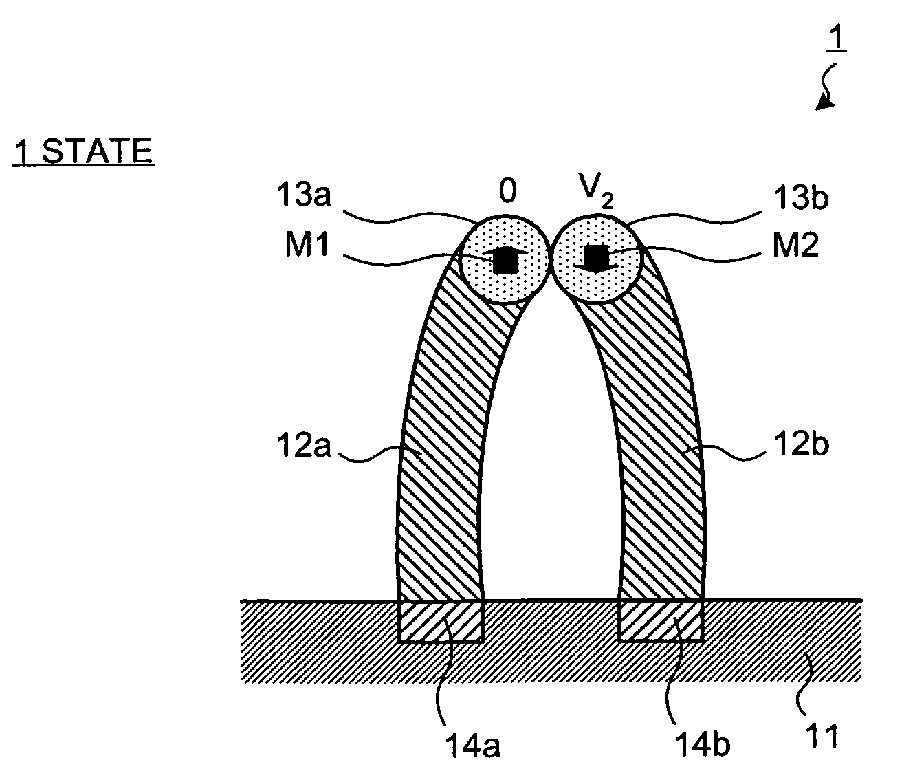
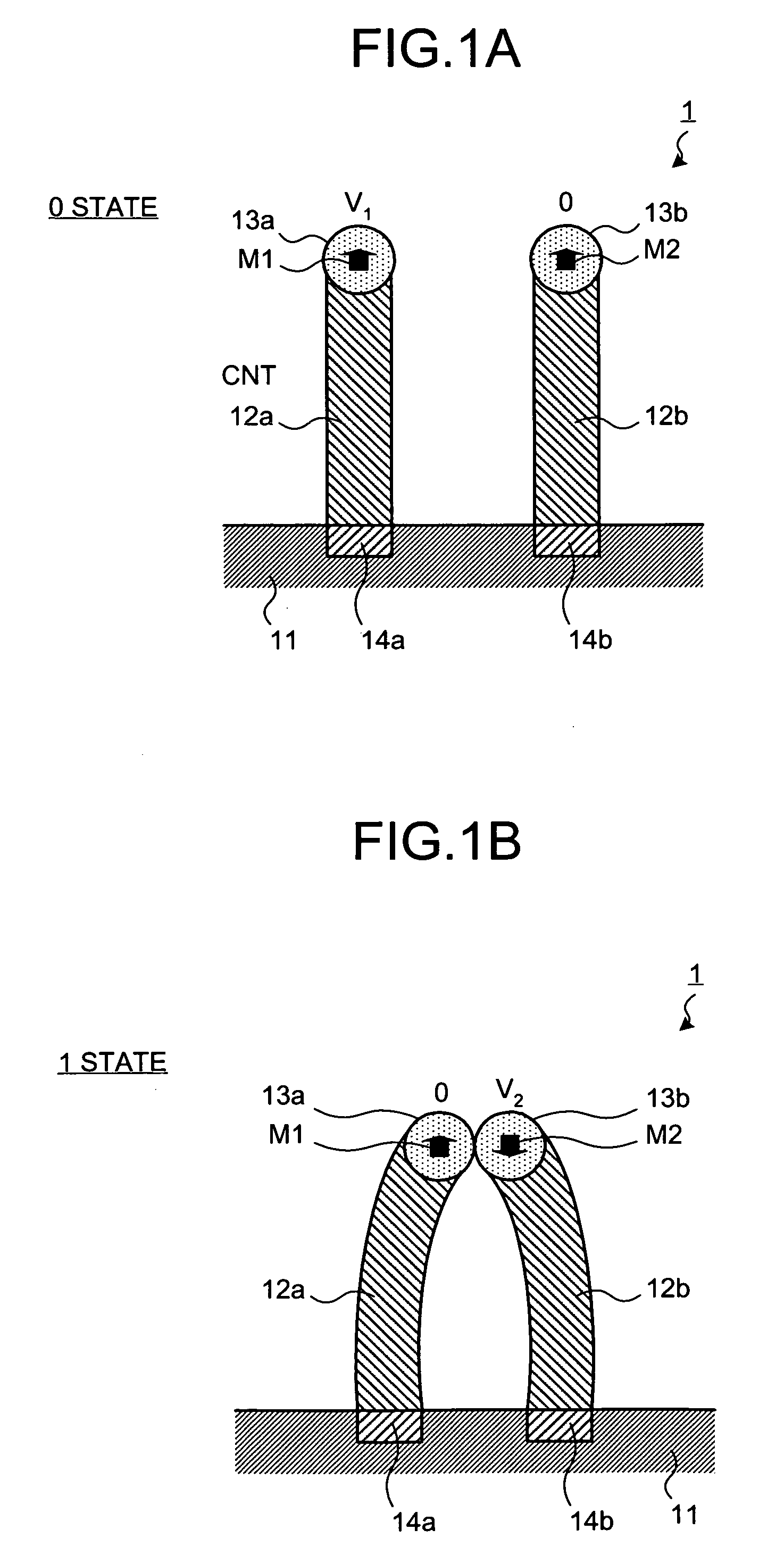
[0146] In the case where the switch element of the second example is designated by symbols of a switch and a diode, the memory element can be expressed by an equivalent circuit shown in FIG. 19. At this time, V4=0.5 V. When the voltage shown in FIG. 19 was applied for input, deletion and reading with respect to a specified cell S, it was confirmed that the memory element operated as RAM (Random Access Memory).

Manufacturing of the Magnetoresistive Effect Element in a Fourth Example

[0147] In the fourth example, the magnetoresistive effect element corresponding to the magnetoresistive effect element in the fourth embodiment was manufactured by the following method.

[0148] Similarly to the switch element in the first example, the aluminum layer was formed as the conductive layers 14a and 14b on the substrate 11, and two carbon nanotubes 12a and 12b where the cobalt particles are provided at their tip ends wer...

fifth embodiment

Confirmation for the Operation of the Magnetoresistive Effect Element in the Fifth Embodiment

[0155] The magnetoresistive ratio of the magnetoresistive effect element in the fifth example manufactured in the above manner was measured similarly to the fourth example. The magnetoresistive ratio was about 50%, and it was found that this was inferior to that of the magnetoresistive effect element in the fourth example. This is because since band discontinuity of silicon oxide (SiO2) with respect to cobalt is larger than that of the titanium oxide (TiO2), magnetization dependency of the tunnel probability becomes small. As a result, it could be confirmed that the tunnel phenomenon is dominant in the magnetoresistive effect elements manufactured in the fourth and fifth examples.

[0156] The switch element according to the present embodiments is effective as the switch element to be used in the field of the electronic devices which require high quality and miniaturization.


PUM

PropertyMeasurementUnit
Young's modulusaaaaaaaaaa
magnetic permeabilityaaaaaaaaaa
heightaaaaaaaaaa

Abstract

A switch element includes a substrate; a plurality of carbon nanotubes provided upright on the substrate; magnetic particles arranged at tip ends of the carbon nanotubes respectively; and a plurality of conductive layers formed between base ends of the carbon nanotubes and the substrate. A switching operation of the switching element is performed in such a manner that the carbon nanotubes or the magnetic particles are brought into contact with each other according to an electrical potential between the conductive layers, and the carbon nanotubes are separated from each other when an electrical current flows through the carbon nanotubes with the carbon nanotubes or the magnetic particles brought into contact with each other.

Description

CROSS-REFERENCE TO RELATED APPLICATIONS [0001] This application is based upon and claims the benefit of priority from the prior Japanese Patent Application No. 2005-234515, filed on Aug. 12, 2005; the entire contents of which are incorporated herein by reference.BACKGROUND OF THE INVENTION [0002] 1. Field of the Invention [0003] The present invention relates to a switch element, a memory element and a magnetoresistive effect element which use carbon nanotube. [0004] 2. Description of the Related Art [0005] Simply, the most notable feature of carbon nanotube is a cylinder made of graphite having a hollow portion. The carbon nanotube can be roughly divided into a single-walled carbon nanotube (CNT; SWCNT) of a one bar shape, and a multi-walled carbon nanotube (Multi-walled CNT; MWCNT) having a concentrically nested structure. Basically, a great difference between them is a difference in diameter, and the diameter of the single-walled CNT is several nm or less, and the diameter of the ...

Claims


Application Information

Patent Timeline
Patent Type & Authority Applications(United States)
IPC IPC(8): H01L21/00
CPCB82Y10/00G11C11/54H01L43/08G11C23/00H01H1/0094G11C13/025Y10S977/762H10N50/10
Inventor YAMAUCHI, TAKASHITANAKA, CHIKASUGIYAMA, HIDEYUKIKINOSHITA, ATSUHIROKOGA, JUNJIMOTOI, YUICHINAKANO, YOSHIHIKOSUENAGA, SEIICHI
Owner KK TOSHIBA
Why Eureka
Try Eureka