An Integrated Electronic Assembly And Method For Conserving Space In A Circuit

Active Publication Date: 2007-02-22
COILCRAFT
View PDF20 Cites 8 Cited by
  • Summary
  • Abstract
  • Description
  • Claims
  • Application Information

AI Technical Summary

Problems solved by technology

These applications further drive technology to research new areas and ideas with respect to miniaturizing electronics and often require “low profile” components due to constraints in height and width.
Unfortunately, the technology is often limited due to the inability to make certain circuits and components smaller, faster, or more powerful.
This technique left half of the PCB unpopulated because one side had to be reserved for solder pads and solder and required enough space on the PCB to mount each individual component.
Many times, however, these options were not available due to constraints in size for the PCBs.
As a result of these advances in technology, current electronic circuits

Method used


Image

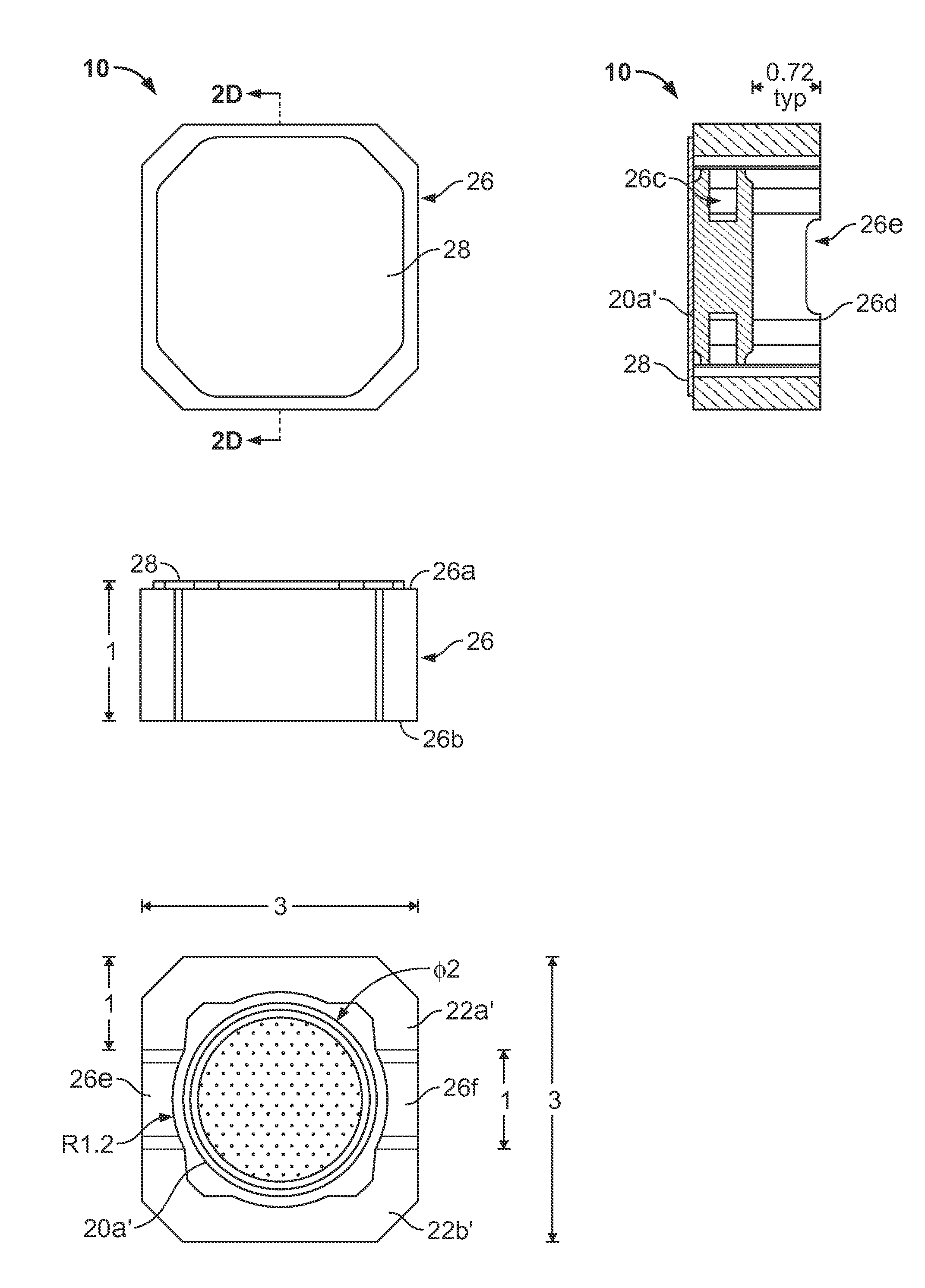
  • An Integrated Electronic Assembly And Method For Conserving Space In A Circuit
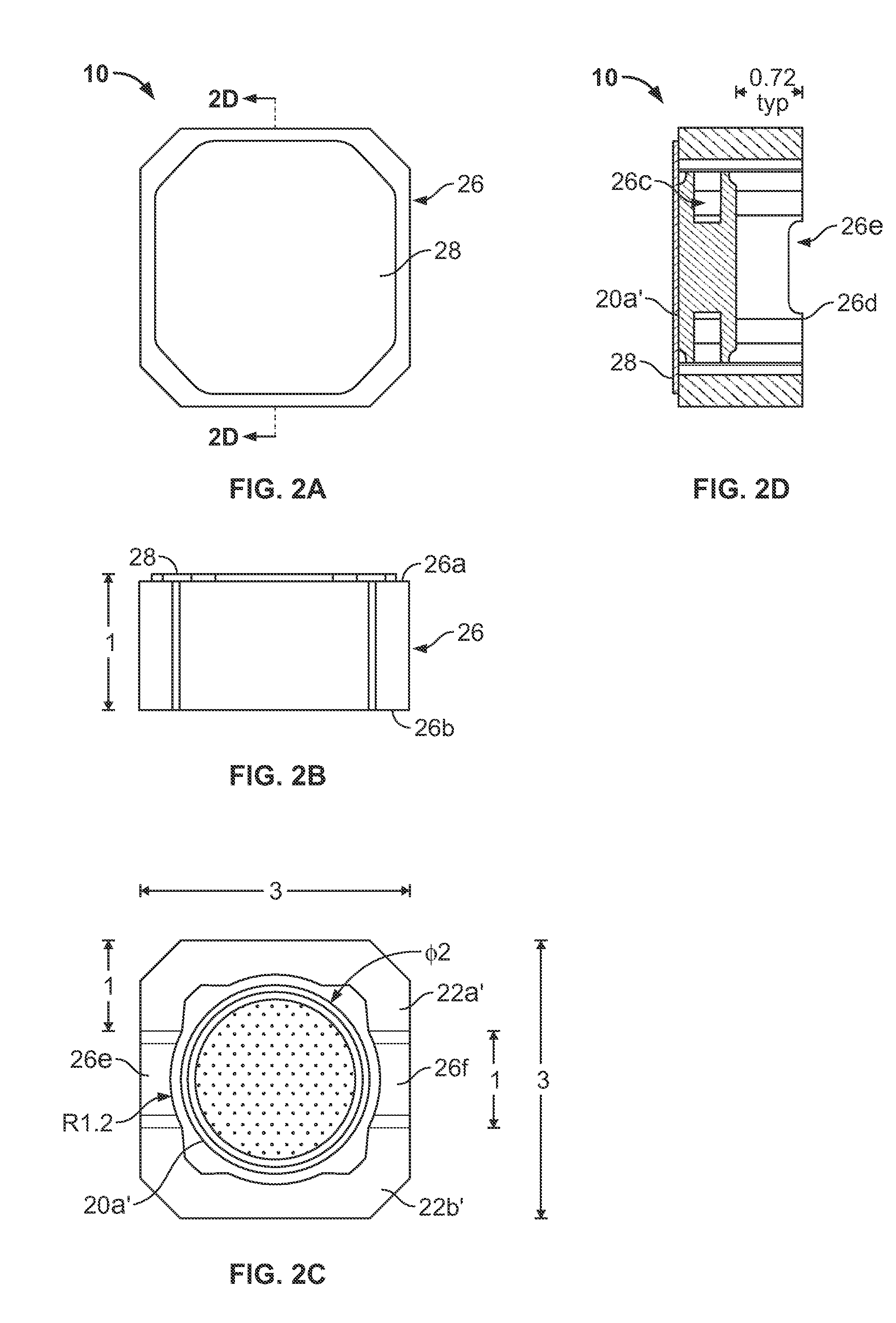
  • An Integrated Electronic Assembly And Method For Conserving Space In A Circuit
  • An Integrated Electronic Assembly And Method For Conserving Space In A Circuit

Examples


Embodiment Construction

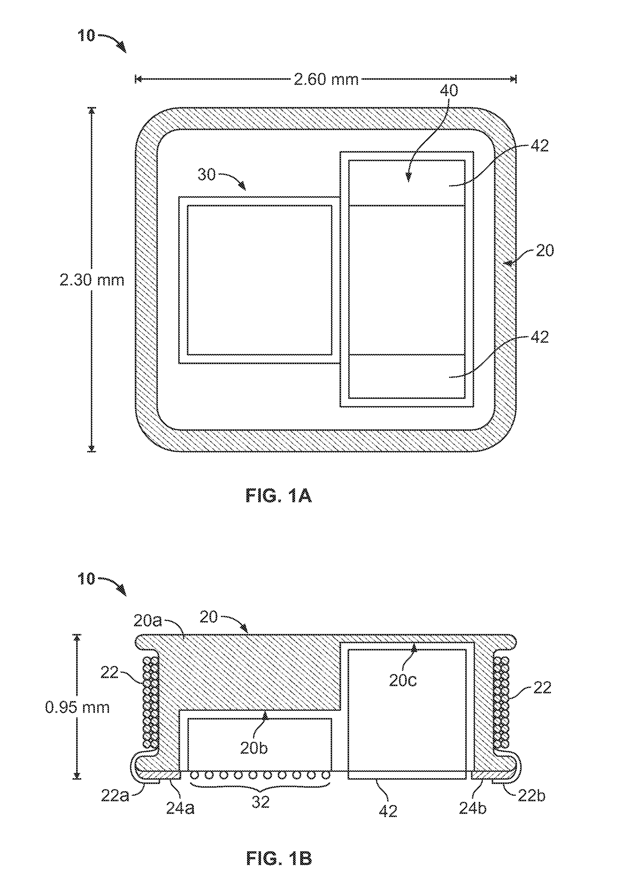
[0019] An integrated electronic assembly in accordance with the invention includes a first electronic component and at least a second electronic component wherein the first electronic component defines a receptacle, such as a recess or opening, into which at least a portion of the second electronic component is disposed. Once the second electronic component is disposed in the opening of the first electronic component, the first and second electronic components collectively form an integrated electronic assembly which may be connected to a substrate, such as a PCB, as a single component or assembly or within the footprint of a single component as will be discussed further below.

[0020] In a preferred form, the first electronic component has a footprint of a specified size for mounting the first electronic component to the PCB and defines a sufficient opening so that the second electronic component can be mounted to the PCB within the footprint of the first electronic component. The f...


PUM

PropertyMeasurementUnit
Sizeaaaaaaaaaa
Currentaaaaaaaaaa

Abstract

An integrated electronic assembly including a first electronic component defining a receptacle and at least a second electronic component wherein at least a portion of the second electronic component is disposed in the receptacle of the first electronic component, and a method for conserving space in a circuit or on a printed circuit board by integrating a plurality of electronic components so that the plurality of electronic components collectively take up a smaller amount of space on a substrate than the plurality of electronic components would if the plurality of electronic components were not integrated.

Description

CROSS-REFERENCE TO RELATED APPLICATION [0001] This application claims the benefit of U.S. Provisional Application No. 60 / 709,491, filed Aug. 19, 2005, which is hereby incorporated herein by reference in its entirety.FIELD OF THE INVENTION [0002] This invention relates generally to electronic components and more particularly concerns integrated electronic assemblies and methods for conserving space in a circuit or on a substrate. BACKGROUND OF THE INVENTION [0003] The electronics industry is continually called upon to make products smaller and more powerful. Applications such as mobile phones, portable computers, computer accessories, hand-held electronics, etc., create a large demand for smaller electronic components. These applications further drive technology to research new areas and ideas with respect to miniaturizing electronics and often require “low profile” components due to constraints in height and width. Unfortunately, the technology is often limited due to the inability ...

Claims


Application Information

Patent Timeline
IPC IPC(8): H01H11/00
CPCH05K1/181H01F5/04H05K5/0095H05K7/005H05K2201/1003H05K2201/10515H05K2201/10537H05K2201/10636H05K2201/10689H05K1/183H05K7/20127H05K2201/10015H05K2201/10166Y10T29/4913Y10T29/49105Y10T29/4902Y10T29/49073Y02P70/611H05K3/341Y02P70/50
Inventor SEDIO, STEPHEN MICHAEL
Owner COILCRAFT
Why Eureka
Try Eureka