

Photomask for double exposure and double exposure method using the same
a double exposure and photomask technology, applied in the field of double exposure photomasks, can solve the problems of defective photomask patterns, deterioration of yields in the manufacture, and difficulty in reducing the line width and line spacing of photomasks below a certain level via single exposure processes, so as to reduce yields and cycle time. , the effect of reducing the yield
- Summary
- Abstract
- Description
- Claims
- Application Information
AI Technical Summary
Benefits of technology
Problems solved by technology
Method used
Image

Examples
Embodiment Construction
[0039] Exemplary embodiments of the present invention will be described in detail with reference to the accompanying drawings.
[0040] A photomask for a double exposure process and a double exposure method using the same according to an embodiment of the invention will be described with reference to the drawings such that those skilled in the art may practice the present invention according to the teachings of the description.
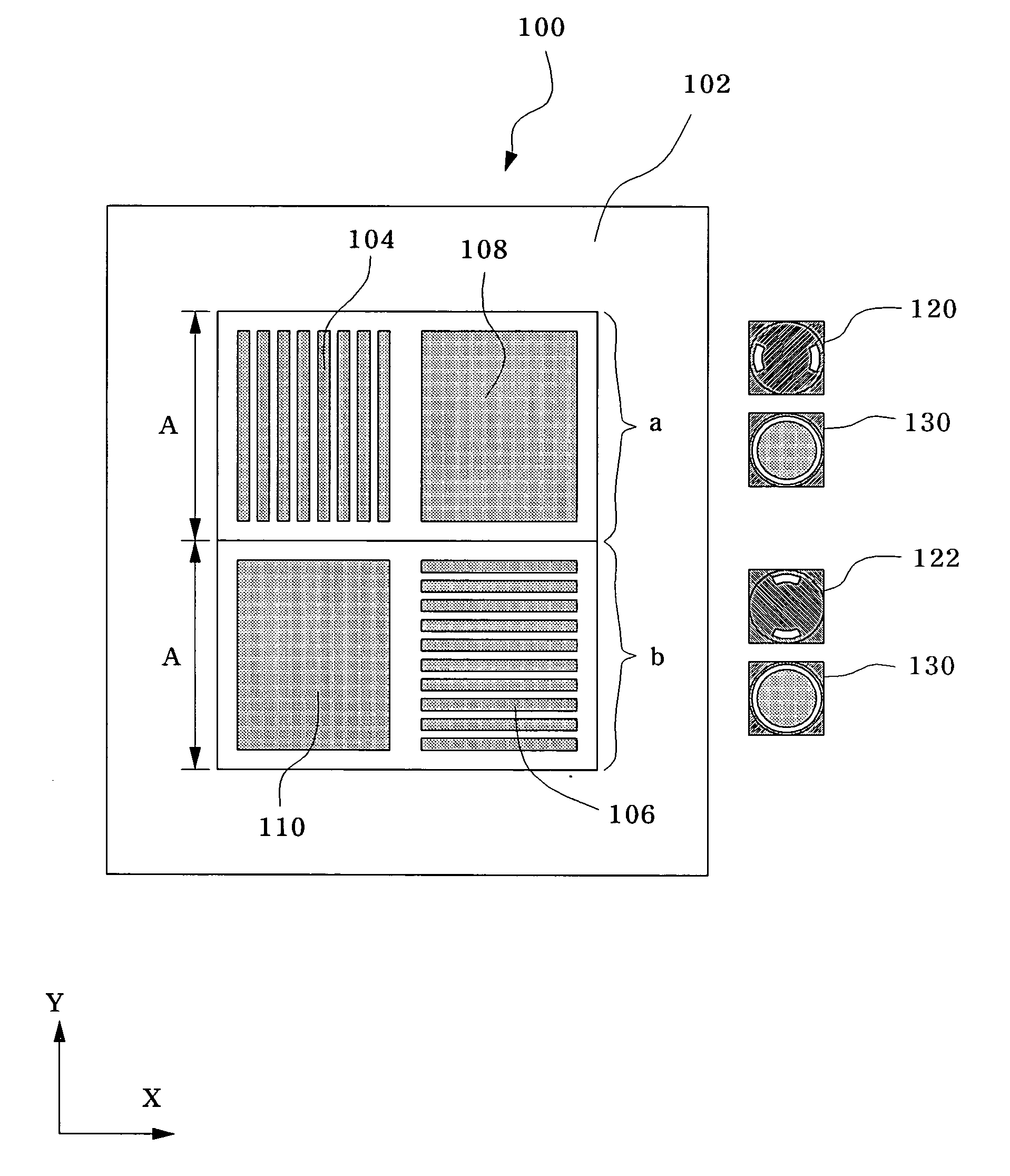
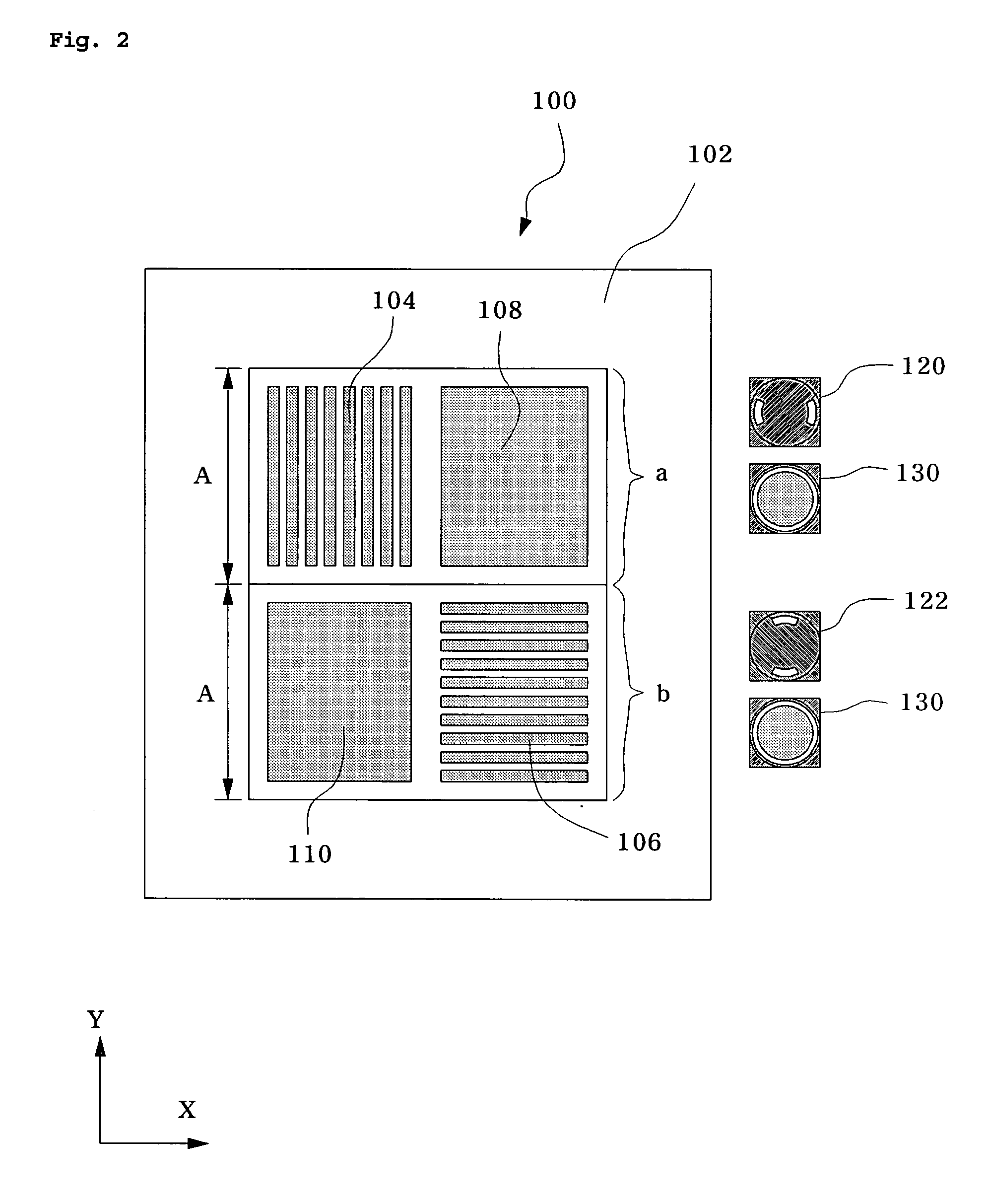
[0041]FIG. 2 is an exemplary simplified schematic view illustrating a photomask for a double exposure process in accordance with a specific embodiment of the invention, and FIG. 6 is an exemplary simplified schematic view illustrating a photoresist pattern formed on a semiconductor wafer after a double exposure process has been performed using the photomasks of FIGS. 2 to 5.
[0042] Referring to FIG. 2, a photomask 100 used in a double exposure process is provided, with photomask 100 being arranged to move in first and second directions. The first and second dir...
PUM
| Property | Measurement | Unit |
|---|---|---|
| density | aaaaa | aaaaa |
| size | aaaaa | aaaaa |
| circuit density | aaaaa | aaaaa |
Abstract
Description
Claims
Application Information