Phosphor, semiconductor light emitting device, and fabrication method thereof
a light emitting diode and semiconductor technology, applied in the direction of luminescent compositions, energy-saving lighting, sustainable buildings, etc., can solve the problems of poor color rendering properties, difficulty in providing crystal growth, and difficulty in realizing a gan-based light emitting diode that can emit light with a wavelength as short as that of ultraviolet light, etc., to achieve excellent color rendering properties, excellent crystallinity, and high brightness
- Summary
- Abstract
- Description
- Claims
- Application Information
AI Technical Summary
Benefits of technology
Problems solved by technology
Method used
Image

Examples
first embodiment
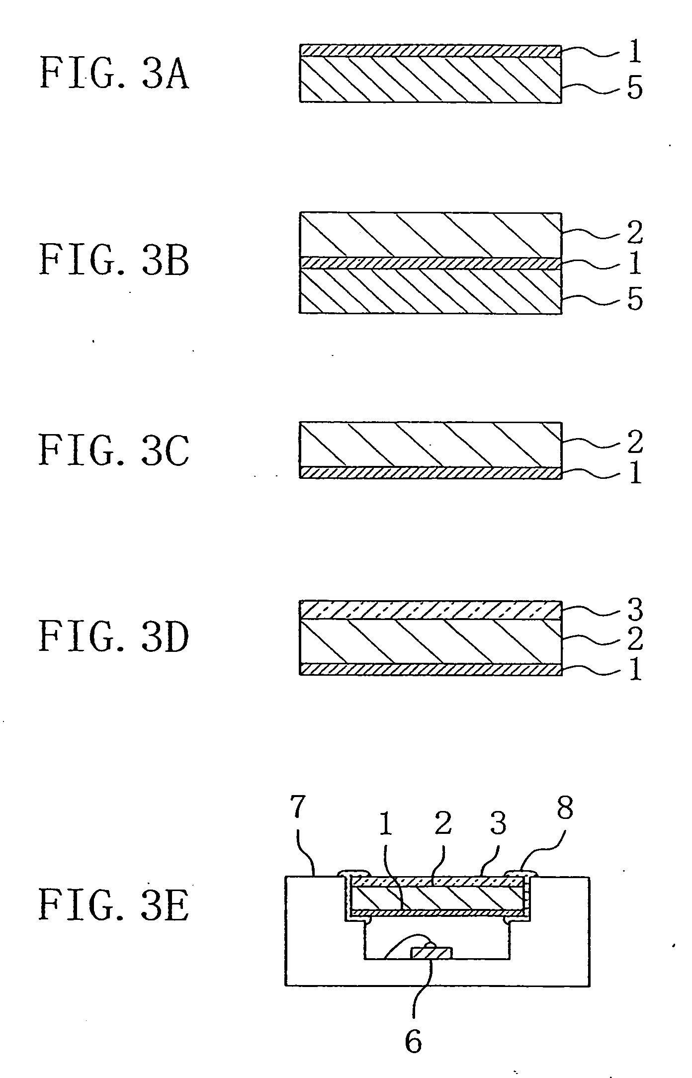
[0108] Hereinafter, a phosphor according to a first embodiment of the present invention will be described with reference to FIG. 1, FIG. 2, and FIGS. 3(a) through 3(e).
[0109] First, the structure of the phosphor according to the first embodiment of the present invention will be described with reference to FIG. 1 and FIG. 2.
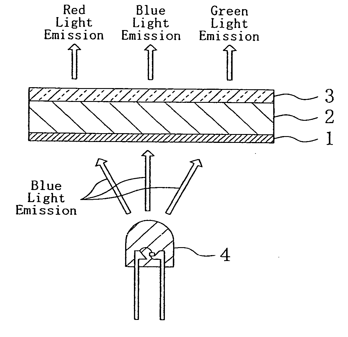
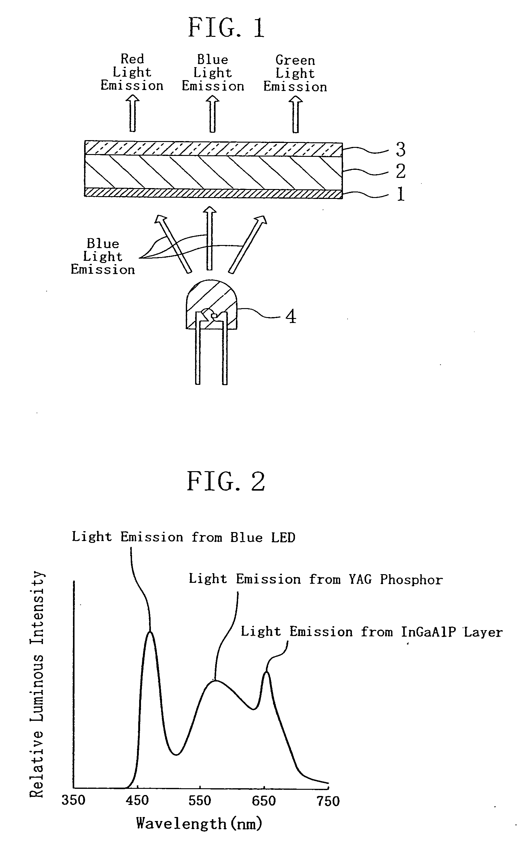
[0110]FIG. 1 is a cross-sectional view illustrating the phosphor according to the first embodiment of the present invention and a blue-light-emitting diode used to excite the phosphor.
[0111] As shown in FIG. 1, an undoped InGaAlP layer 1 that emits red light due to excitation by a blue-light-emitting diode 4 is pasted on one principal surface of a quartz substrate 2, while a YAG phosphor 3 that emits yellow light due to excitation by the blue-light-emitting diode 4 is formed on the other principal surface of the quartz substrate 2.
[0112] Thus, the phosphor according to the first embodiment of the present invention has the structure made up of the InGaAlP layer...
second embodiment
[0124] Hereinafter, a phosphor according to a second embodiment of the present invention will be described with reference to above-mentioned FIGS. 3(a) through 3(e), FIG. 4 and FIG. 5.
[0125] First, the structure of the phosphor according to the second embodiment of the present invention will be described with reference to FIG. 4.
[0126]FIG. 4 is a cross-sectional view illustrating the phosphor according to the second embodiment of the present invention and an ultraviolet-light-emitting diode used to excite the phosphor.
[0127] As shown in FIG. 4, an undoped InGaAlP layer 1 that emits red light due to excitation by an ultraviolet-light-emitting diode 11 is pasted on one principal surface of a quartz substrate 2, while a green-light-emitting phosphor 9 that emits green light due to excitation by the ultraviolet-light-emitting diode 11 and a blue-light-emitting diode 10 that emits blue light due to excitation by the ultraviolet-light-emitting diode 11 are formed in this order over the...
third embodiment
[0141] Hereinafter, a phosphor according to a third embodiment of the present invention will be described with reference to above-mentioned FIG. 5, FIG. 6, and FIGS. 7(a) through 7(d).
[0142] First, the structure of the phosphor according to the third embodiment of the present invention will be described with reference to FIG. 6.
[0143]FIG. 6 is a cross-sectional view illustrating the phosphor according to the third embodiment of the present invention and an ultraviolet-light-emitting diode used to excite the phosphor.
[0144] As shown in FIG. 6, a ZnMgSSe layer 14 that emits blue light due to excitation by an ultraviolet-light-emitting diode 11, an undoped second InGaAlP layer 13 that emits green light due to excitation by the ultraviolet-light-emitting diode 11, and an undoped first InGaAlP layer 12 that emits red light due to excitation by the ultraviolet-light-emitting diode are formed in this order over one principal surface of a quartz substrate 2.
[0145] Thus, the phosphor acc...
PUM
| Property | Measurement | Unit |
|---|---|---|
| band gap | aaaaa | aaaaa |
| wavelength | aaaaa | aaaaa |
| thickness | aaaaa | aaaaa |
Abstract
Description
Claims
Application Information
 - R&D Engineer
- R&D Manager
- IP Professional
- Industry Leading Data Capabilities
- Powerful AI technology
- Patent DNA Extraction
Browse by: Latest US Patents, China's latest patents, Technical Efficacy Thesaurus, Application Domain, Technology Topic.
© 2024 PatSnap. All rights reserved.Legal|Privacy policy|Modern Slavery Act Transparency Statement|Sitemap