[0006]It is found that, in order to form a light emitting device emitting white light by using, for example, a light emitting device emitting blue light and resins containing light color conversion members as described above, it is most preferable to deposit resins containing light color conversion members directly around a LED chip without mixing each light color conversion member, for improving external
quantum efficiency. However, since a size of the LED chip is very small such as approximately 0.3
millimeter cube, it is very difficult to deposit, for example, a resin containing green color conversion member and a resin containing red color conversion member separately and with a desired quantity. Then, the present inventor studied and examined earnestly and repeatedly, and, as a result, it is found that, by attaching a resin containing a light color conversion member to a transfer pin and transferring it on a side of a light emitting element chip, the resin can be deposited without mixing of the resin containing red color conversion member and the resin containing green color conversion member, and with a precise adjustment of a quantity which can be achieved by adjusting a thickness of the transfer pin, and both resins can be deposited directly even on a small chip and almost independently, thereby a white semiconductor light emitting device with very high external
quantum efficiency can be obtained.
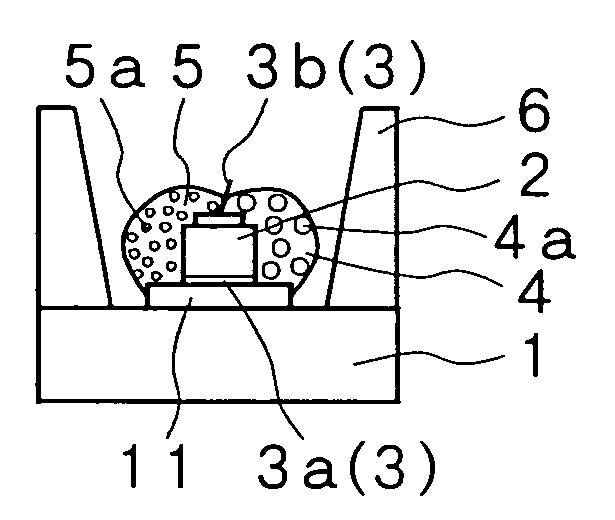
[0011]It is preferable that at least one of the connection means is constituted of a wire which connects one
electrode of the light emitting element chip and one of the pair of the electrode films or the first and second leads, and the first resin layer and the second resin layer are formed divided approximately by a dividing plane which is perpendicular to a surface of the light emitting element chip in a direction of extending the wire, because an accident such that a wire is touched and broken during forming the first resin layer and the second resin layer is easily prevented.
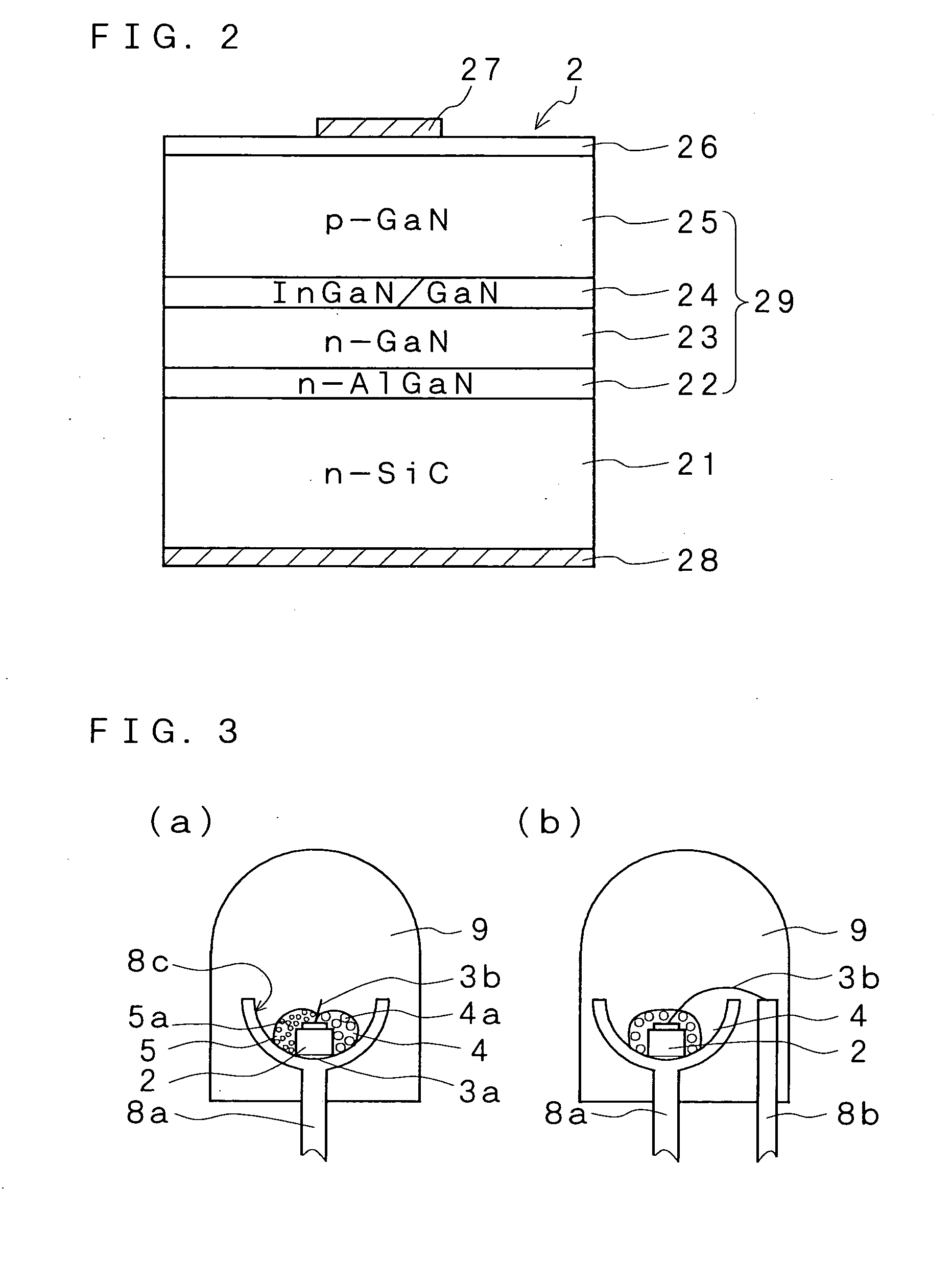
[0015]It is preferable that a wire is bonded on at least one of the electrodes of the light emitting element chip, and the first and second resin layers are formed by contacting the transfer pins with the light emitting element chip from both sides of the wire, because the transfer pin is easily prevented from contacting with the wire.
[0017]According to the aspect of the present invention in which each substantially half is coated with a resin, since the resin containing the light color conversion member is directly deposited around the light emitting element chip, blue light emitted by the light emitting element chip can be converted by a small quantity of the light color conversion member. In addition, since the resin containing the red color conversion member and the resin containing the green color conversion member are provided on each substantially half of the light emitting element chip separately, light color once converted into green is not converted into red again and conversion into very stable light color can be achieved. Here, although both of the resins are partially overlapped at their border portion, by depositing the resin containing a red color conversion member first, even if light is converted into red light and the red light transmits through a green color conversion member, the light converted into red light can not be converted into green light again since the green color conversion member does not absorb and transmits light having smaller
band gap energy than that of the green color conversion member, namely light having a longer
wavelength than that of green color. As a result, a part of light emitted from the light emitting element chip emitting blue light is converted into red light and green light, and white light is obtained by mixing with blue light which is not converted by both light color conversion members. And, since the light color conversion member is minimized, a white semiconductor light emitting device can be formed with small attenuation of light, very high external
quantum efficiency, stable light color and good color rendering property.
[0020]By the manufacturing method by
coating the resin according to the present invention, since the resin is deposited by the transfer method in which a transfer pin is contacted directly with a side or angle part of the light emitting element chip, a depositing quantity or a depositing position can be adjusted very precisely by adjusting a thickness of the transfer pin. As a result, a quantity of a minimum essential of the resin can be deposited, useless absorption of the light decreases, and the white light emitting device with remarkably high external
quantum efficiency can be obtained. In addition, even in case that the wire exists on the surface of the light emitting element chip, since the transfer pin can be brought close to the light emitting element chip from the sides interposing the wire, the resin can be deposited without contacting the transfer pin with the wire, reliability of the wire can be improved.

