BGA package with stacked semiconductor chips and method of manufacturing the same

a technology of semiconductor chips and stacked packages, which is applied in the direction of semiconductor devices, semiconductor/solid-state device details, electrical apparatus, etc., can solve the problems of increasing the thickness of the overall semiconductor package, hindering the manufacture of thinner semiconductor packages, and solder balls for connecting packages being exposed to an external environment, so as to achieve less expensive mass production and more reliable results

Inactive Publication Date: 2007-03-22
SAMSUNG ELECTRONICS CO LTD
View PDF6 Cites 28 Cited by
  • Summary
  • Abstract
  • Description
  • Claims
  • Application Information

AI Technical Summary

Benefits of technology

[0014] The exemplary embodiments of the present invention provide a BGA package with stacked semiconductor chips, which is thinner and / or more reliable and / or permits less expensive mass production.

Problems solved by technology

However, conventional packages with stacked semiconductor chips may have the following disadvantages.
This leads to an increase in the thickness of the overall semiconductor packages, which may hinder the manufacture of thinner semiconductor packages.
Second, solder balls for connecting packages may be exposed to an external environment.
That is, because portions for connecting packages are not molded by an EMC, the reliability of the conventional package with stacked semiconductor chips may be degraded after using the package for many hours.
Further, a conductive post disclosed in Korean Patent Laid-open Publication No. 2002-0043435 may be inadequate for mass production considering the manufacturing cost and / or process complexity.

Method used


Image

  • BGA package with stacked semiconductor chips and method of manufacturing the same
  • BGA package with stacked semiconductor chips and method of manufacturing the same
  • BGA package with stacked semiconductor chips and method of manufacturing the same

Examples


Embodiment Construction

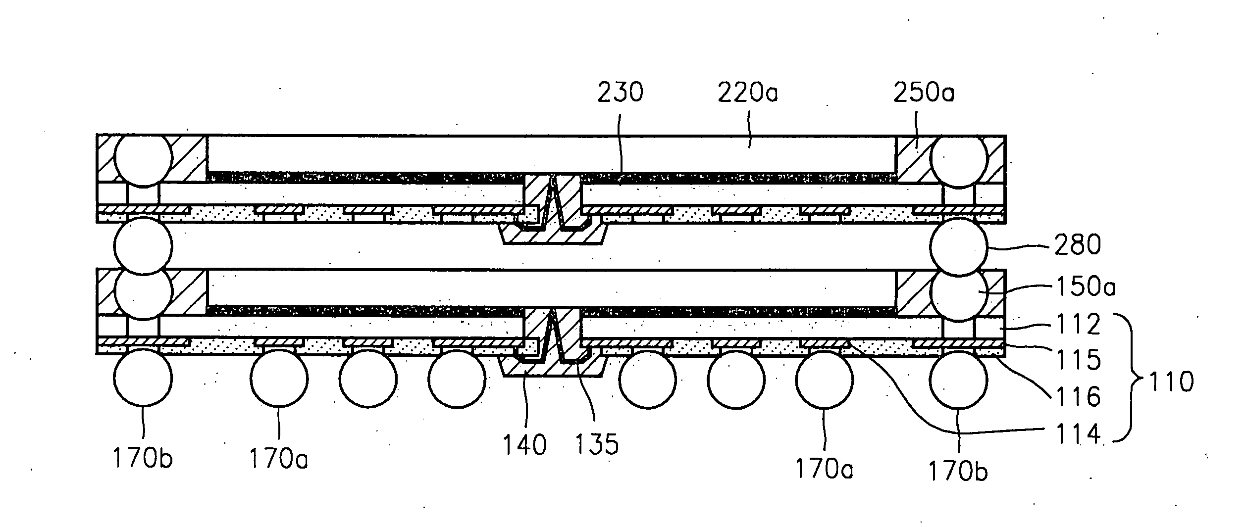
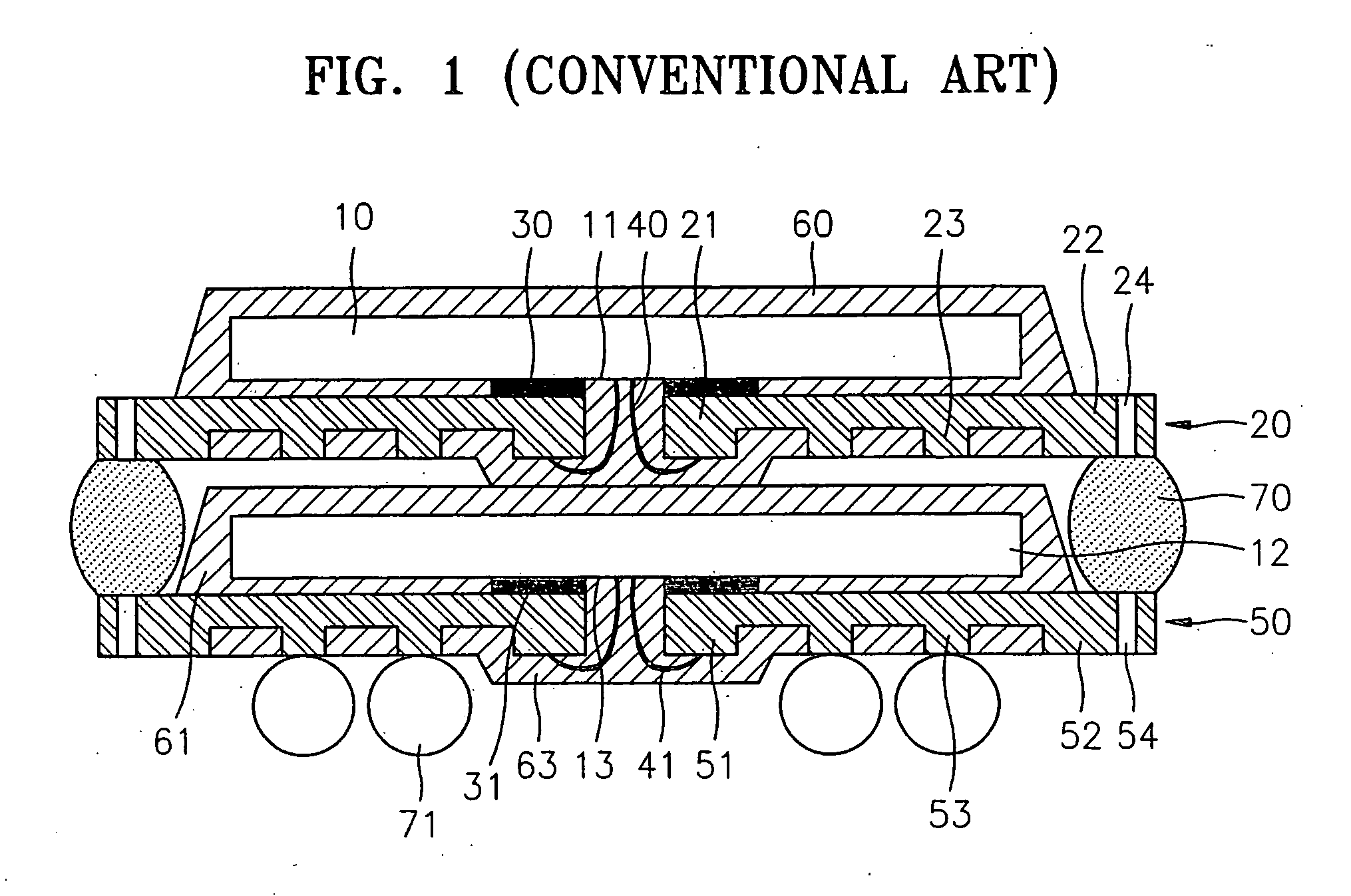
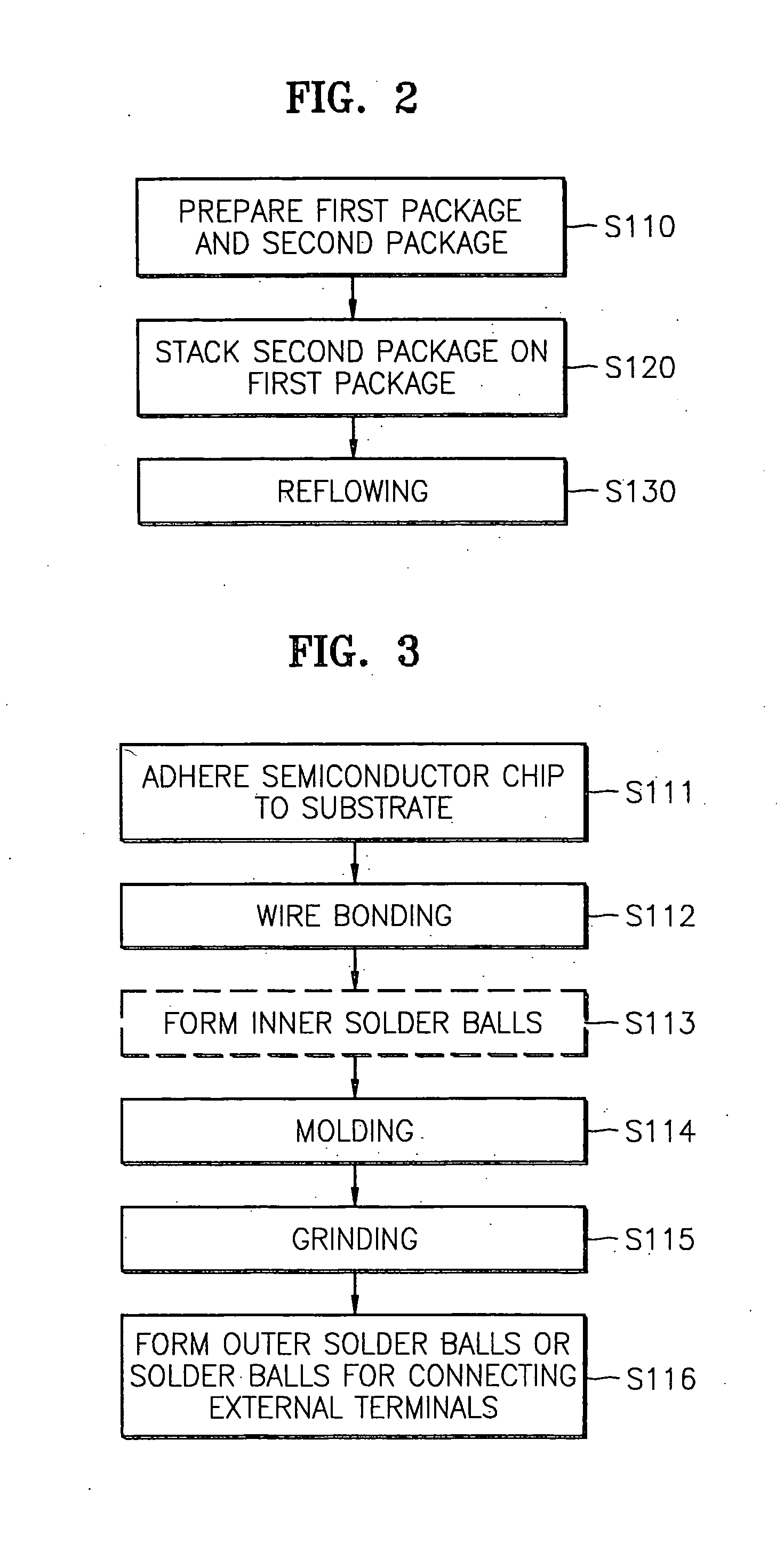
[0032] The present invention will now be described more fully with reference to the accompanying drawings, in which exemplary embodiments of the invention are shown. However, the present invention may be embodied in many different forms and should not be construed as being limited to the exemplary embodiments set forth herein. Rather, these exemplary embodiments are provided for the purpose of illustration; the present invention covers various changes in form and details as will be readily contemplated by those ordinarily skilled in the art.

[0033] It should also be noted that the thicknesses of various layers and regions in the stacked package have been exaggerated in the drawings for the purpose of clarity and the same drawing reference numerals are used for the same elements even in different drawings.

[0034] It should also be noted that a layer is considered as being formed “on” another layer or substrate when formed either directly on the referenced layer or the substrate or fo...


PUM


Abstract

A package with two or more stacked semiconductor chips and a method of manufacturing the same. In the method, an upper semiconductor chip package and a lower semiconductor chip package are prepared. Solder balls are formed on a substrate of the lower package to connect the upper and lower packages. A semiconductor chip and the solder balls are molded and then ground until the solder balls are exposed. Solder balls are formed on the bottom of a substrate of the upper package. The upper package is stacked on the lower package such that the solder balls of the lower package are in contact with the solder balls of the upper package. A reflow process is performed on the lower package and the upper package, which are stacked, to physically connect the upper and lower packages.

Description

[0001] This application claims the benefit of priority of Korean Patent Application No. 2003-49137, filed on Jul. 18, 2003, in the Korean Intellectual Property Office, the disclosure of which are herein incorporated by reference in their entirety by reference. BACKGROUND OF THE INVENTION [0002] 1. Field of the Invention [0003] The present invention relates to a semiconductor package, and more particularly, to a ball grid array (BGA) package with two or more stacked semiconductor chips and a method of manufacturing the same. [0004] 2. Description of the Related Art [0005] A semiconductor chip packaging process may be a process of manufacturing semiconductor chips. Semiconductor chip packages may be used to electrically connect semiconductor chips to external apparatuses, protect the semiconductor chips from external enviroment by molding, and / or to dissipate heat. There are a variety of methods of electrically connecting semiconductor chips to external apparatuses; a BGA packaging pr...

Claims


Application Information

Patent Timeline
Patent Type & Authority Applications(United States)
IPC IPC(8): H01L23/02H01L23/31H01L23/12H01L23/48H01L25/065H01L25/07H01L25/10H01L25/18
CPCH01L23/3128H01L25/105H01L2924/07802H01L2224/32225H01L2224/32245H01L2924/15321H01L2225/1058H01L2225/1023H01L2224/45144H01L24/48H01L2924/18165H01L2924/15331H01L2924/15311H01L2924/01079H01L2224/73215H01L2224/4826H01L2224/4824H01L2224/48091H01L2924/00014H01L2924/00H01L24/45H01L2924/181H01L2224/05599H01L23/48
Inventor GO, JUN-YOUNGJUN, BYUNG-SEOKKIM, JAE-HONG
Owner SAMSUNG ELECTRONICS CO LTD
Why Eureka
Try Eureka