Method for integrating a SONOS gate oxide transistor into a logic/analog integrated circuit having several gate oxide thicknesses

a technology of gate oxide transistor and logic/analog integrated circuit, which is applied in the direction of semiconductor devices, basic electric elements, electrical equipment, etc., can solve the problems of dramatic change in the thickness of the top siosub>2 /sub>layer b, and achieve the effects of simple manufacturing process, improved reliability and cost-effectiveness

Active Publication Date: 2005-09-20
CHARTERED SEMICONDUCTOR MANUFACTURING
View PDF12 Cites 116 Cited by
  • Summary
  • Abstract
  • Description
  • Claims
  • Application Information

AI Technical Summary

Benefits of technology

[0012]Still another objective of this invention is to provide a simple manufacturing process that is more reliable and more cost effective.
[0013]This invention provides a method of controlling and minimizing the variation in thickness of the top oxide on a polysilicon / silicon oxide / silicon nitride / silicon oxide / silicon substrate (SONOS) device. This method of minimizing the thickness variation of the top oxide is achieved by using a thin sacrificial Si3N4 layer on the top of a silicon oxide / silicon nitride / silicon oxide (ONO) stacked layer. The sacrificial Si3N4 layer protects the top SiO2 layer from thickness variations on the SONOS devices during the formation of first and second gate oxides on other portions of the substrate.

Problems solved by technology

Unfortunately, during processing to form the first and second gate oxides, the effects of cleaning and oxidizing can dramatically alter the thickness of the top SiO2 layer 20′.

Method used


Image

  • Method for integrating a SONOS gate oxide transistor into a logic/analog integrated circuit having several gate oxide thicknesses
  • Method for integrating a SONOS gate oxide transistor into a logic/analog integrated circuit having several gate oxide thicknesses
  • Method for integrating a SONOS gate oxide transistor into a logic/analog integrated circuit having several gate oxide thicknesses

Examples


Embodiment Construction

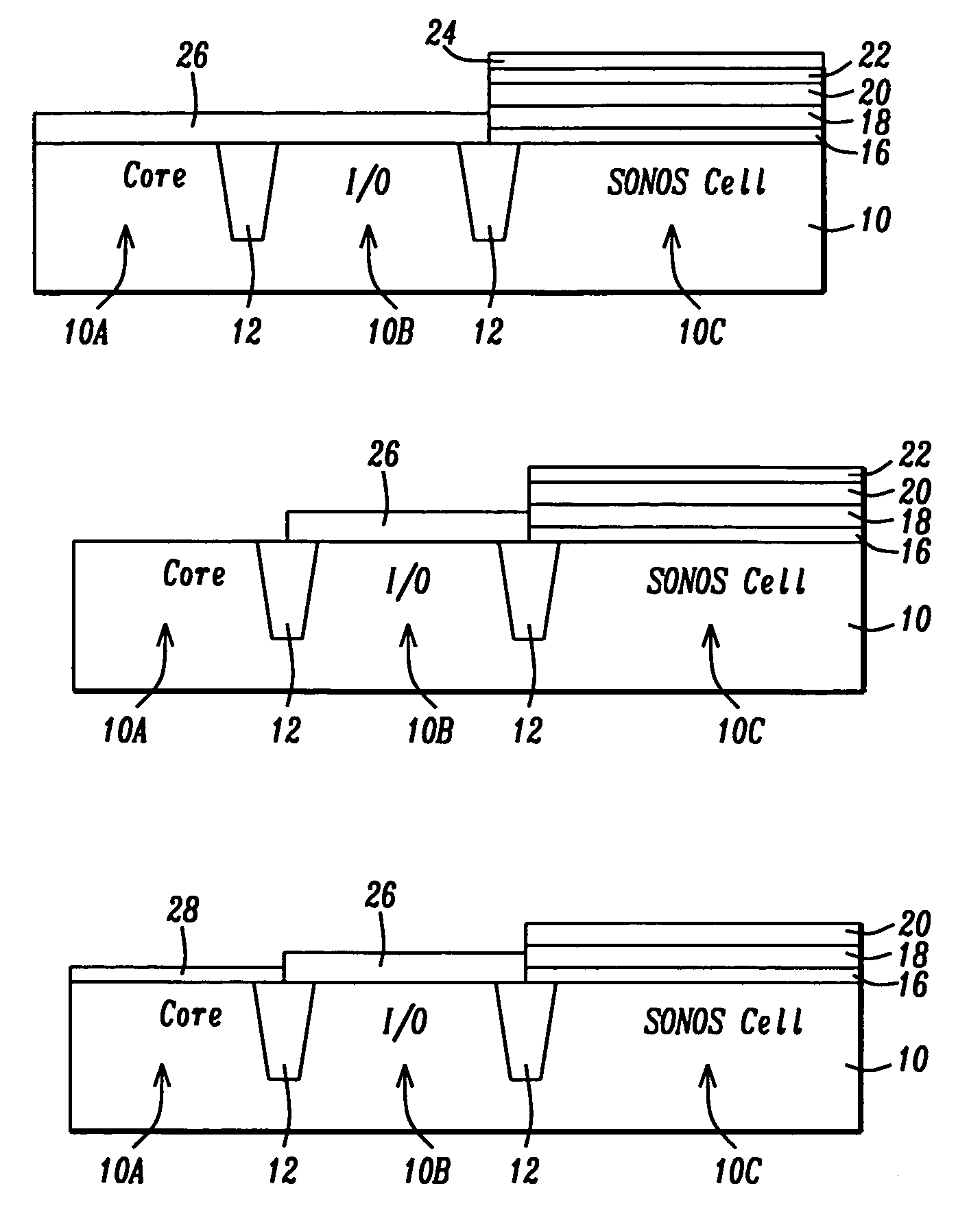
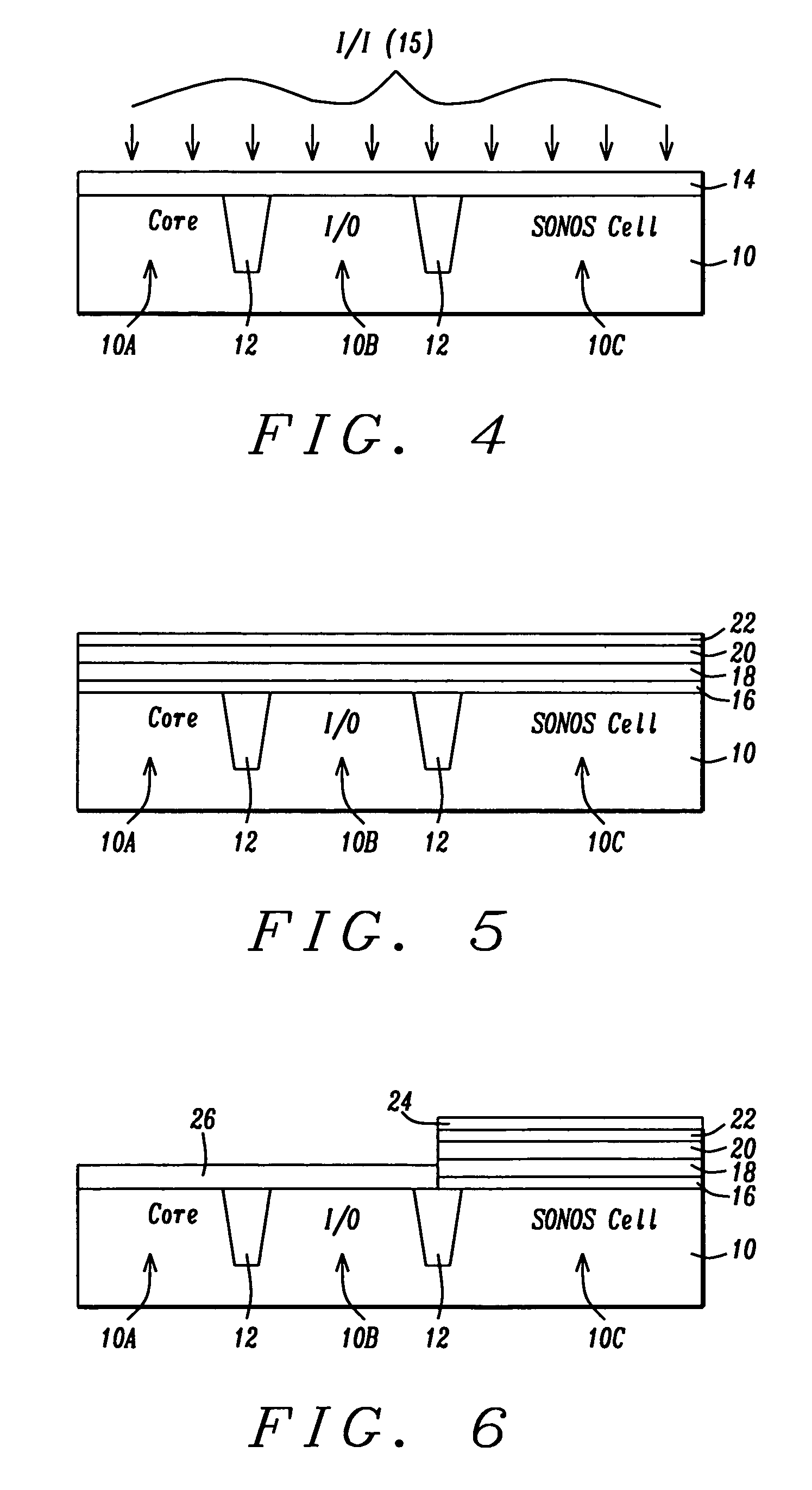
[0021]The method is now described in detail by a first embodiment for making a SONOS storage device with a top oxide having minimum loss and variation while making gate oxides of two different thicknesses on the same substrate. Although this invention is described for a planar gate structure, it is also applicable to non-planar structures such as dual-sidewall gate structures and the like.

[0022]Referring now to FIG. 4, the method begins by providing a substrate 10 having logic (core) regions 10A for logic circuits, I / O regions 10B, and SONOS cell areas (non-volatile memory) 10C. Although the device regions are shown adjacent to each other to simplify the drawings, the actual distribution of these regions depends on the circuit design (layout). The different regions are typically electrically isolated from each other by using shallow trench isolation 12. An implant sacrificial layer 14 is deposited or formed on the substrate 10 for implanting the wells and channels. Sacrificial layer...


PUM


Abstract

A method for integrating a SONOS device with an improved top oxide with SiO2 gate oxides of different thickness is described. In a first embodiment during ISSG oxidation to form the SiO2 gate oxides, a thin sacrificial silicon nitride layer is used over the top oxide of the ONO to minimize loss and to control the top oxide thickness. In a second embodiment the top oxide layer for the SONOS device is formed by depositing an NO stack. During ISSG oxidation to form the SiO2 gate oxides a portion of the Si3N4 in the NO stack is converted to SiO2 to form the top oxide with improved thickness control.

Description

BACKGROUND OF THE INVENTION[0001](1) Field of the Invention[0002]This invention relates to semiconductor integrated circuit devices, and more particularly to a method for controlling the top oxide thickness on a polysilicon / silicon oxide / silicon nitride / silicon oxide / silicon substrate (SONOS) transistor while forming gate oxides of different thicknesses elsewhere on the substrate by a first and second embodiment. The method and structure are particularly suitable for integrating merged logic / analog integrated circuits with non-volatile memory devices.[0003](2) Description of the Prior Art[0004]Merging semiconductor logic / analog devices with non-volatile memory devices is finding extensive use in the electronics industry. These embedded SONOS devices require FETs with different gate oxide thicknesses to optimize the FET performance. Typically non-volatile memory (SONOS) and peripheral input / output (I / O) devices require thicker gate oxides, while CMOS logic / analog devices require a th...

Claims


Application Information

Patent Timeline
Patent Type & Authority Patents(United States)
IPC IPC(8): H01L21/70H01L21/8234H01L21/8238H01L21/8246H01L27/105
CPCH01L21/823462H01L21/823857H01L27/105H01L27/11568H01L27/11573Y10S438/981Y10S438/954H10B43/30H10B43/40
Inventor LEE, JAE GONKOH, HWA WENGQUEK, ELGINSOHN, DONG KYUN
Owner CHARTERED SEMICONDUCTOR MANUFACTURING
Why Eureka
Try Eureka