

Method of resin-seal-molding electronic component and apparatus therefor
a technology of electronic components and resins, which is applied in the direction of electrical equipment, basic electric elements, semiconductor devices, etc., can solve the problems of inability to efficiently release molded products, inability to bond to the surface of the mold for resin molding, and damage to the molded product body (resin-seal-molded body). , to achieve the effect of simplifying the mold structur
- Summary
- Abstract
- Description
- Claims
- Application Information
AI Technical Summary
Benefits of technology
Problems solved by technology
Method used
Image

Examples
first embodiment
[0075]FIGS. 1-14 show a resin-seal-molding apparatus of the present invention. FIG. 1 schematically shows a configuration of a resin-seal-molding apparatus for implementing the resin-seal-molding method, and FIGS. 2-14 schematically show substantial part of a resin-seal-molding portion in the resin-seal-molding apparatus.
[0076]FIGS. 15-20 show a resin-seal-molding apparatus of another embodiment of the present invention.
[0077] First Embodiment
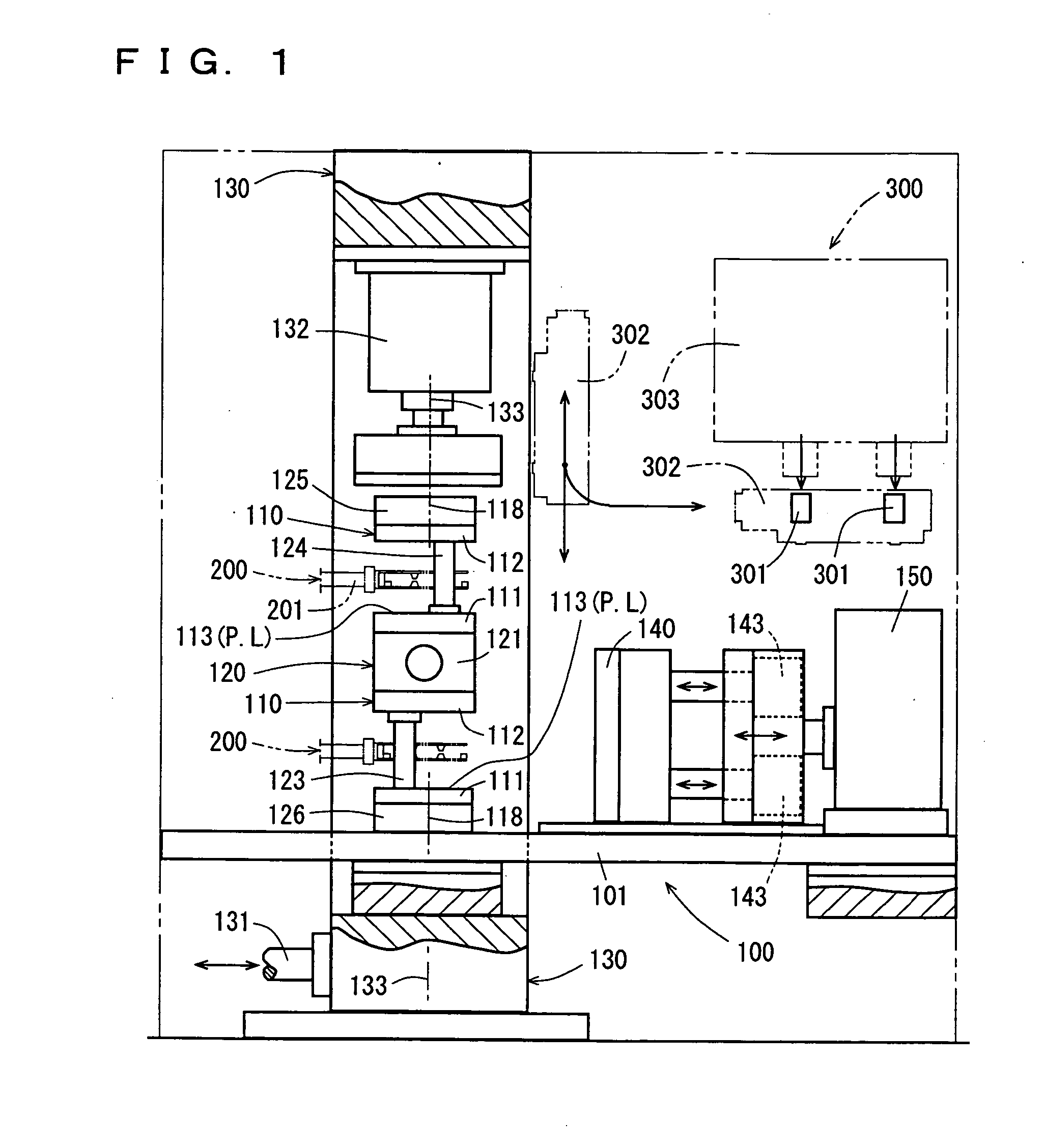
[0078]FIG. 1 schematically shows an overall configuration of a resin-seal-molding apparatus.
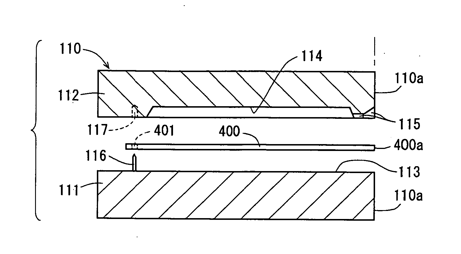
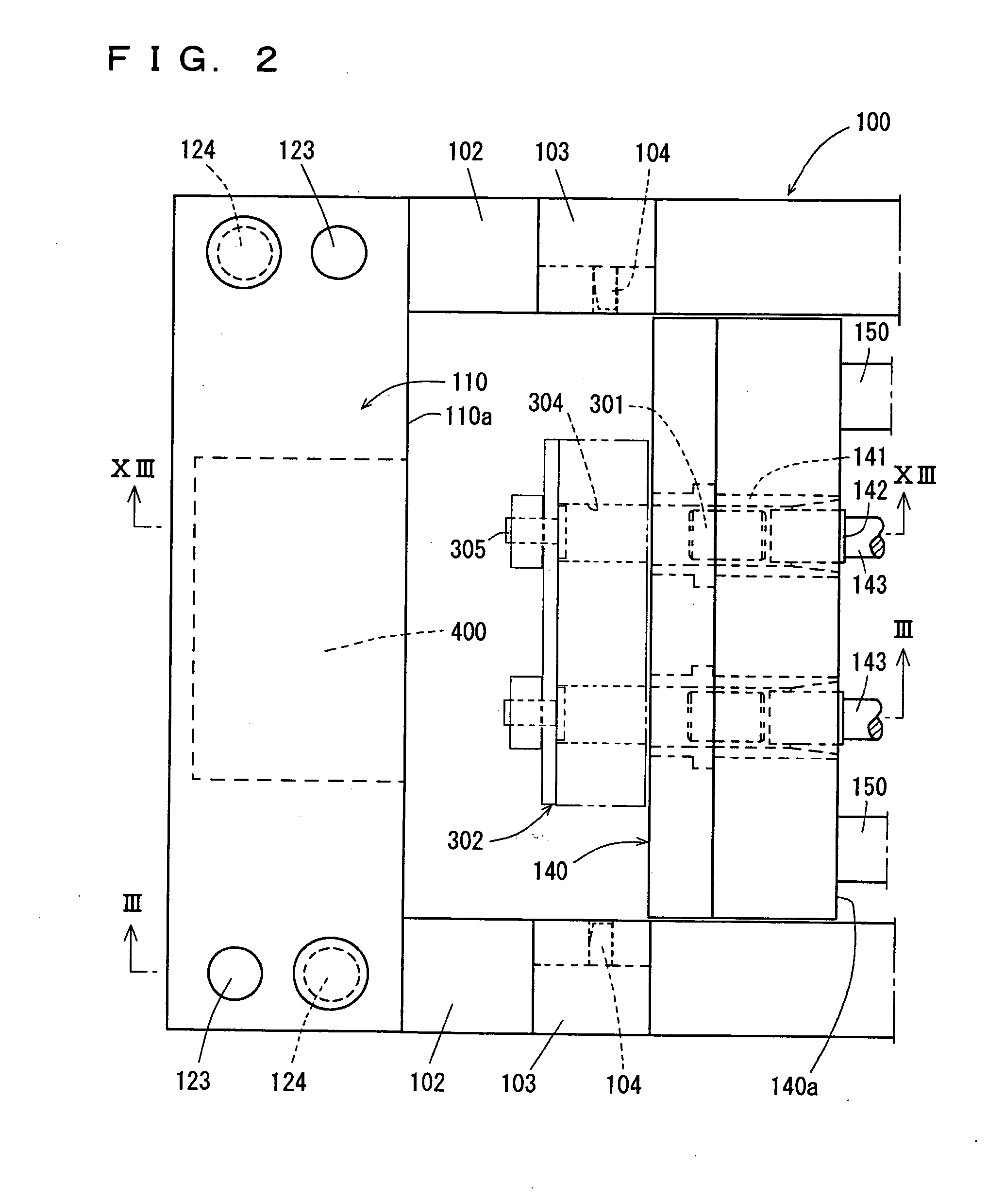
[0079] The resin-seal-molding apparatus includes a resin-seal-molding portion 100 for resin-seal-molding an electronic component on a substrate, a substrate supply-remove mechanism 200 for carry-supplying the before-resin-seal-molding substrate to a prescribed position, which will be described later, of the resin-seal-molding portion and for removing and carrying the resin-seal-molded substrate out of the resin-seal-molding portion, and a resin materi...
second embodiment
[0127] Second Embodiment
[0128]FIGS. 15-17 show a resin-seal-molding apparatus of another embodiment of the present invention, which is different from the resin-seal-molding apparatus of the first embodiment in the following points.
[0129] That is, while the resin-seal-molding apparatus of the first embodiment is provided with one resin-seal-region for resin-sealing an electronic component on one main surface of one substrate 400 (see FIG. 7), the resin-seal-molding apparatus of the present embodiment shown in FIG. 15 is provided with a plurality of resin-seal-regions (two in the illustrated example). Further, the apparatus of the present embodiment is different from the apparatus of the first embodiment in that it is provided with resin material supplying pots 141, resin material pressing plungers 142, and plunger reciprocate drive mechanisms 143 in the number corresponding to the aforementioned plurality of resin-seal-regions.
[0130] While the apparatus shown in FIG. 16 has basical...
third embodiment
[0133] Third Embodiment
[0134]FIGS. 18 and 19 show a resin-seal-molding apparatus of another embodiment of the present invention, which is a modification of the resin-seal-molding apparatus of the second embodiment shown in FIGS. 15 and 16.
[0135] According to the apparatus of the second embodiment shown in FIGS. 15 and 16, the number of resin-seal-molded products that can be obtained from one substrate can be increased. According to the apparatus of the third embodiment shown in FIGS. 18 and 19, the number can further be increased.
[0136] In the apparatus shown in FIG. 18, the apparatus of the second embodiment shown in FIG. 15 is arranged on each side of right and left in the drawing symmetrically. In the apparatus shown in FIG. 19, the apparatus shown in FIG. 16 is arranged on each side of right and left in the drawing symmetrically.
[0137] In the apparatus of the third embodiment, the clamping pressure is individually applied to each of molds 110 arranged symmetrically. According...
PUM
| Property | Measurement | Unit |
|---|---|---|
| clamping pressure | aaaaa | aaaaa |
| size | aaaaa | aaaaa |
| adhesion | aaaaa | aaaaa |
Abstract
Description
Claims
Application Information