Image forming apparatus

Inactive Publication Date: 2007-04-19
KYOCERA DOCUMENT SOLUTIONS INC
View PDF1 Cites 12 Cited by
  • Summary
  • Abstract
  • Description
  • Claims
  • Application Information

AI Technical Summary

Benefits of technology

[0033] With this construction, it is possible to perform the correction accurately even when a next round of image formation is requested

Problems solved by technology

This breaks the balance of electric discharge between the charger and the photoconductor drum, increasing the potential on the surface of the photoconductor.
Disadvantageously, this significantly affects image quality such as color reproducibility in low-density portions and in a color copier.
This increases the resistance of the grid again, and thus increases the surface potential of the photoconductor.
By the methods disclosed in JP-A-

Method used


Image

  • Image forming apparatus
  • Image forming apparatus
  • Image forming apparatus

Examples


Example

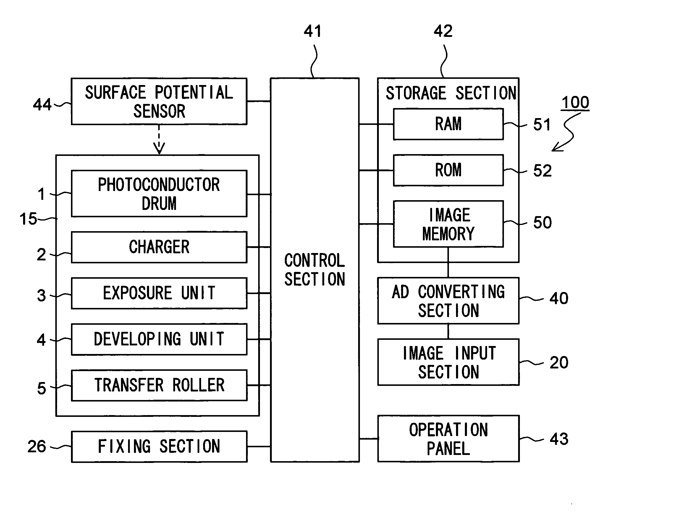
[0056]FIG. 2 is a block diagram showing the configuration of the image forming apparatus of a first embodiment of the present invention. Such parts as are found also in FIG. 1 are identified with common reference numerals. The image forming apparatus 100 includes the image forming section 15, the image input section 20, an AD converting section 40, a control section 41, a storage section 42, an operation panel 43, a surface potential sensor 44, and other components.

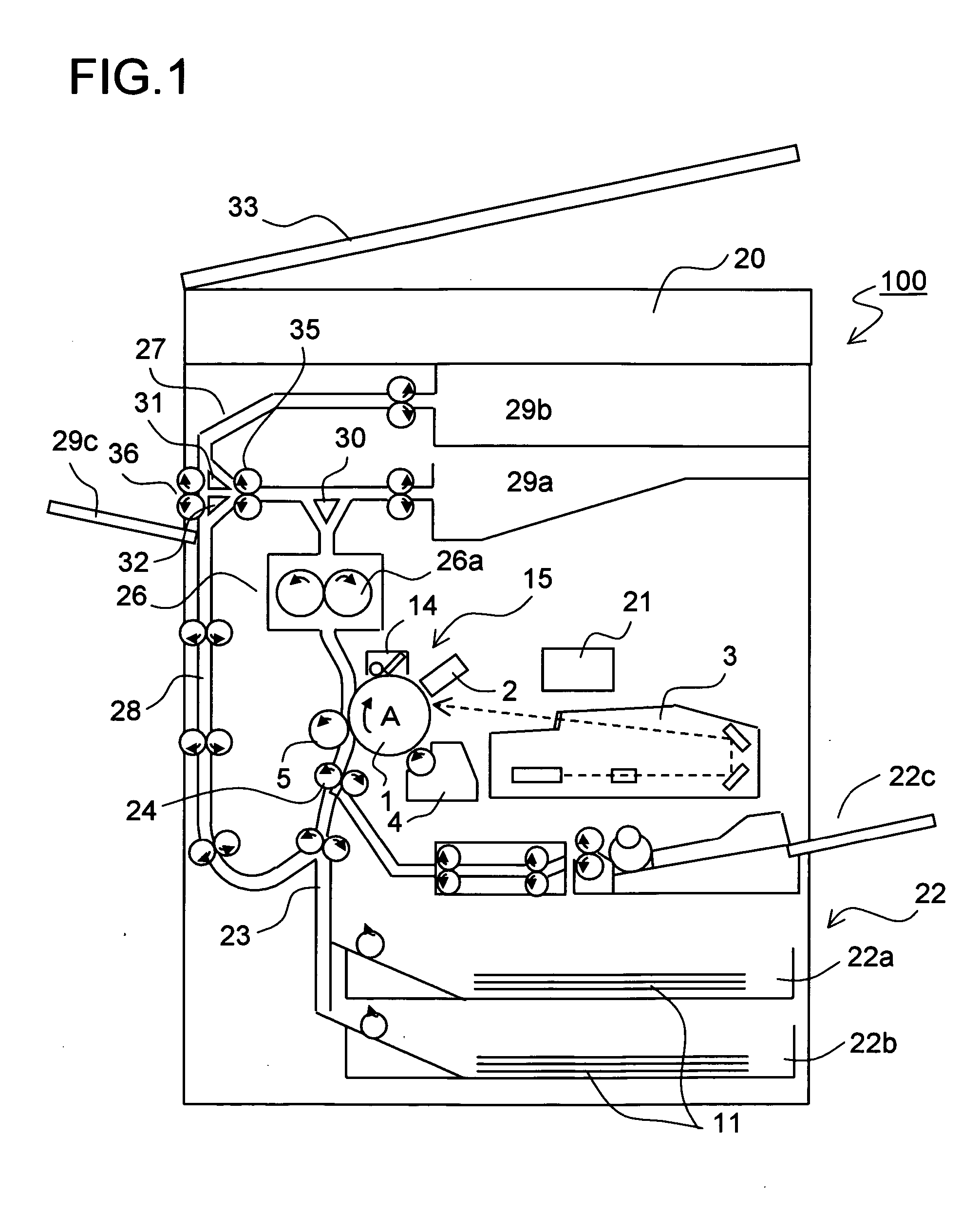
[0057] In a case where the image forming apparatus 100 is a copier as shown in FIG. 1, the image input section 20 is an image reading section that is composed of: a scanning optical system that includes a scanner lamp that illuminates an original document at the time of copying and mirrors that deflect the optical path of the reflected light from the original document; a condenser lens that focuses the reflected light from the original document to form an image; a CCD that converts the thus focused image light into elect...

Example

[0092]FIG. 9 is a block diagram showing the configuration of the image forming apparatus of a second embodiment of the present invention. Such parts as are found also in FIG. 2 are identified with common reference numerals. As compared with the image forming apparatus of the first embodiment, the image forming apparatus 100 here is provided with, instead of the surface potential sensor 44, a printed sheet counter 45 that counts the total number of printed sheets in the image forming section 15. In other respects, the configuration here is the same as in the first embodiment, and hence no description thereof will be repeated.

[0093] This embodiment is characterized in that, based on the total number of printed sheets as counted from the initial state of the apparatus by the printed sheet counter 45, the reference value is set for the adjustment of the surface potential of the photoconductor, and the first correction is performed based on a predetermined correction amount per unit num...

Example

[0120]FIG. 14 is a flowchart showing how the image forming apparatus of the third embodiment operates. Now, the image forming process of the image forming apparatus will be described according to the steps shown in FIG. 14 with reference to FIGS. 1, 12, 13A, 13B and 13C. First, the humidity inside the apparatus is detected with the humidity sensor 46 (step S1), and the humidity thus detected is stored as an initial humidity in the storage section 42. Next, whether or not image formation is requested by a user is checked (step S2), and, if image formation is requested, the total number of printed sheets is calculated by the printed sheet counter 45 (step S3) and then the control section 41 reads the reference value Ga corresponding to the calculation result from the reference value data that has previously been stored in the storage section 42 (step S4).

[0121] The humidity inside the apparatus is detected anew with the humidity sensor 46 (step S5) so that, based on the difference be...


PUM


Abstract

In an image forming apparatus, a control section 41 adjusts the surface potential of a photoconductor or the developing potential of a developer carrying member based on the detection result of a surface potential sensor 44, and performs first correction whereby, relative to the reference value of the applied bias of a charger 2 or the developing bias of the developer carrying member in a developing unit 4 as observed during potential adjustment, the applied bias or the developing bias is varied so as to keep constant the potential difference between the surface potential of the photoconductor and the developing potential of the developer carrying member during image formation. The control section also performs second correction whereby the applied bias or the developing bias is restored to the reference value over a predetermined period after the completion of continuous image formation.

Description

[0001] This application is based on Japanese Patent Application No. 2005-301298 filed on Oct. 17, 2005 and Japanese Patent Application No. 2006-21810 filed on Jan. 31, 2006, the contents of which are hereby incorporated by reference. BACKGROUND OF THE INVENTION [0002] 1. Field of the Invention [0003] The present invention relates to an electrophotographic image forming apparatus incorporating a photoconductor, and more particularly to a method of stabilizing the potential on the surface of the photoconductor or the developing potential of a developer carrying member. [0004] 2. Description of Related Art [0005] The construction of the image forming section of a conventional image forming apparatus is shown in FIG. 15. In FIG. 15, along the direction of rotation (indicated by arrow A) of a photoconductor drum 1, the image forming section 15 is fitted with a charger 2, an exposure unit 3, a developing unit 4, a transfer roller 5, a scrubbing roller 6, a cleaning blade 9 and a charge el...

Claims


Application Information

Patent Timeline
IPC IPC(8): G03G15/02G03G15/06
CPCG03G15/5037G03G2215/00054
Inventor SAKATO, SHINGOTAKAGAMI, AINIMURA, EIJIHAMAKAWA, HIROYUKIHORIUCHI, YOSHINORIFUJISHIMA, MASASHI
Owner KYOCERA DOCUMENT SOLUTIONS INC
Why Eureka
Try Eureka