Semiconductor module including a plurality of IC chips therein

a technology of ic chips and semiconductors, applied in the field of semiconductor modules, can solve problems such as error or malfunction, distortion of the original rectangular waveform of the common signal,

Inactive Publication Date: 2007-04-26
RENESAS TECH CORP +2
View PDF9 Cites 28 Cited by
  • Summary
  • Abstract
  • Description
  • Claims
  • Application Information

AI Technical Summary

Benefits of technology

[0013] In view of the above problems in the conventional technique, it is an object of the present invention to provide a semiconductor module wherein the length of the interconnect lines disposed between IC chips can be adjusted without increasing the number of interconnect layers in the wiring board.

Problems solved by technology

This may cause a distortion of the original rectangular waveform of the common signal, and incur an error or malfunction in operation of the semiconductor module 40.

Method used


Image

  • Semiconductor module including a plurality of IC chips therein
  • Semiconductor module including a plurality of IC chips therein
  • Semiconductor module including a plurality of IC chips therein

Examples


first embodiment

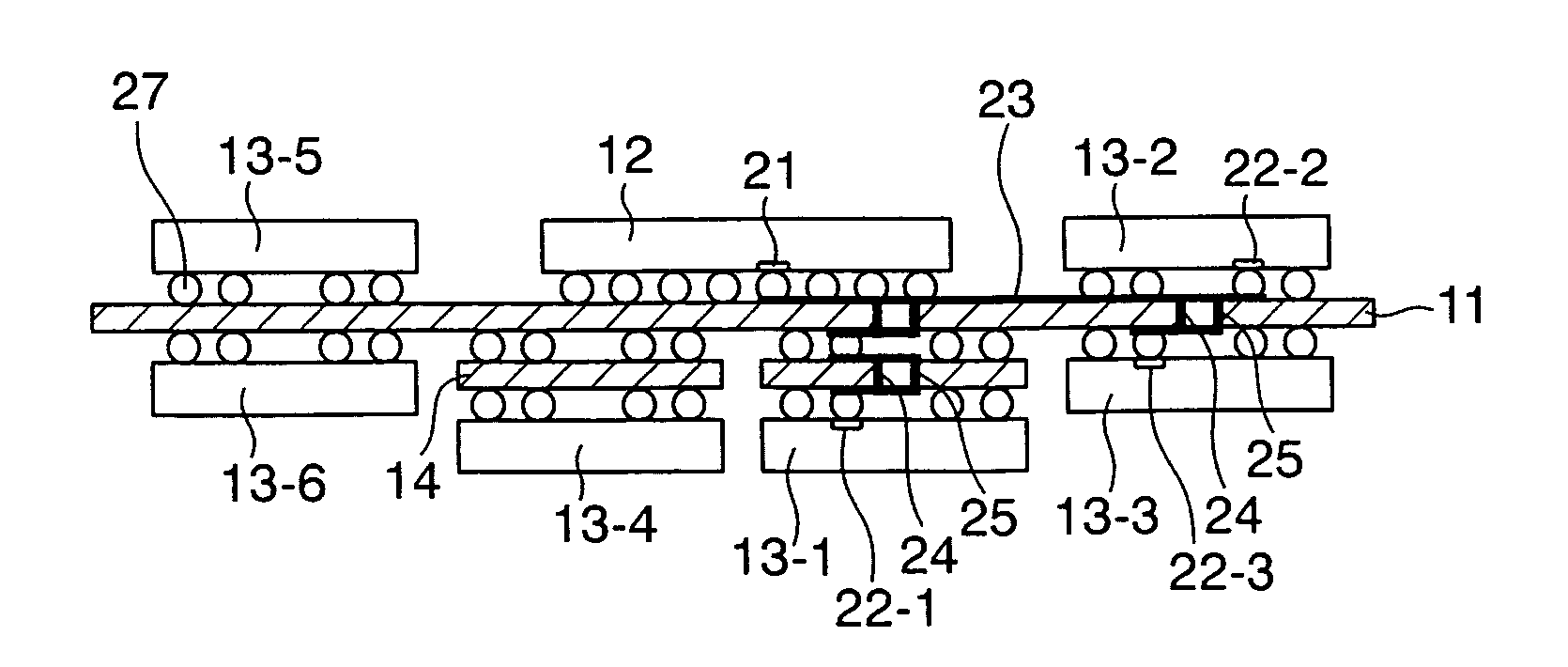
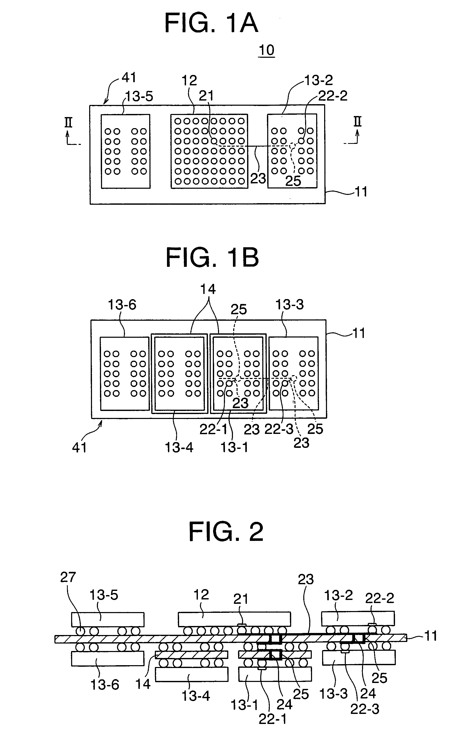
[0030]FIGS. 1A and 1B show a semiconductor module according to the present invention. The semiconductor module, generally designated by numeral 10, includes a wiring board 11, such as a printed circuit board, a driver chip (driver IC chip) 12, a plurality of memory chips (memory IC chips) 13 driven by the driver chip 12, and a plurality of interposer substrates 14 interposing between the wiring board 11 and some of the memory chips 13.

[0031] The driver chip 12 is disposed on the central area of the top surface of the wiring board 11, and the memory chips 13 (13-1 to 13-6) are disposed on / above the top and bottom surfaces of the wiring board 11 in a symmetric arrangement. In the present embodiment, two memory chips 13-1 and 13-4 are mounted on the central area of the bottom surface of the wiring board 11 with an intervention of the respective interposer substrates 14. The driver chip 12 and other memory chips 13-2, 13-3, 13-5 and 13-6 are directly mounted on the wiring board 11.

[003...

third embodiment

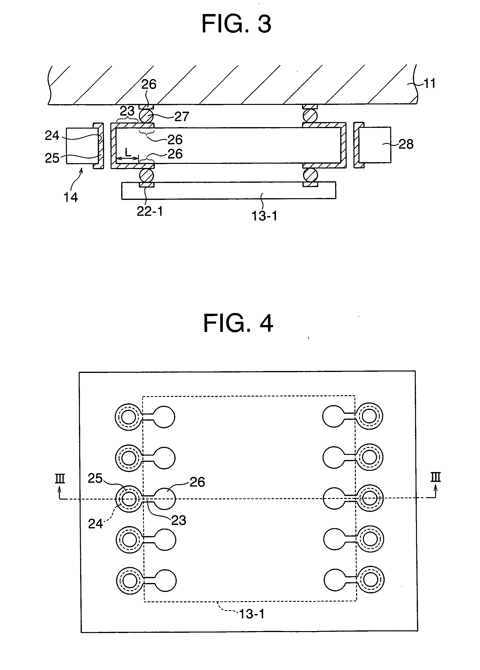
[0047]FIG. 8 is a sectional view of a semiconductor module according to the present invention, showing the vicinity of the interposer substrate. The interposer substrate 14 in the present embodiment has a plurality (3) of insulation layers 28 and four interconnect layers including top and bottom interconnect layers. The top and bottom interconnect layers each include address signal lines 23, address signal terminals 26a, ground terminal 26b. Via-holes 24a and 24b are disposed in the vicinity of the address signal terminals 26a and the ground terminals 26b, respectively, and receive therein via-lines 25a and 25b.

[0048] Interconnect lines 23a, 23b connect terminals 26a, 26b and via-lines 25a, 25b together on both top and bottom surfaces. Two interconnect layers 29 sandwiched between adjacent insulation layers 28 connect to ground via-lines 25b to thereby configure the interconnect layers 29 as reference layers or ground layers. The reference layers 29 are formed as a substantially pl...


PUM


Abstract

A semiconductor module includes a driver IC chip and a plurality of memory IC chips on a common wiring board. Some of the memory IC chips nearer to the driver IC chip than the other memory IC chips are mounted on an interposer substrate mounted on the wiring board, providing a uniform line length among a species of signal lines for the memory IC chips.

Description

BACKGROUND OF THE INVENTION [0001] (a) Field of the Invention [0002] The present invention relates to a semiconductor module and, more particularly, to a semiconductor module including a plurality of IC chips mounted on a wiring board. [0003] (b) Description of the Related Art [0004] In a typical semiconductor module, a common wiring board, such as a printed circuit board, mounts thereon a plurality of IC chips which are connected together by interconnect lines formed within the wiring board. FIGS. 11A and 11B exemplify the top and bottom surfaces, respectively, of a conventional semiconductor module including a plurality of memory IC chips. [0005] The semiconductor module, generally designated by numeral 40, includes a driver IC chip 12 and a plurality of memory IC chips 13 (13-1 to 136) driven by the driver IC chip 12, all of which are mounted on a common wiring board 211. The driver IC chip 12 is mounted at the center of the top surface of the wiring board 11, whereas the memory ...

Claims


Application Information

Patent Timeline
Patent Type & Authority Applications(United States)
IPC IPC(8): H01L23/52
CPCH01L23/5385H01L25/0652H01L2924/3011H05K1/0237H05K1/181H05K2201/049H05K2201/10159H05K2201/10378H05K2201/10734H05K2203/1572H01L2224/16225H01L2224/05571H01L2224/05573H01L2924/00014H01L2224/0615Y02P70/50H01L2224/05599
Inventor IWASAKI, HIRONORIONO, TAKAO
Owner RENESAS TECH CORP
Why Eureka
Try Eureka