Method of fabricating interconnect structure

a technology of interconnection and structure, which is applied in the direction of electrical equipment, semiconductor devices, semiconductor/solid-state device details, etc., can solve the problems of unfavorable physical properties of porous low-k layers, and unfavorable interconnection line pitch

Active Publication Date: 2007-04-26
UNITED MICROELECTRONICS CORP
View PDF8 Cites 6 Cited by
  • Summary
  • Abstract
  • Description
  • Claims
  • Application Information

AI Technical Summary

Benefits of technology

[0008] In view of the foregoing, this invention provides an interconnect structure to prevent the above-mentioned accumulative effect caused by multiple UV-curing cycles.
[0018] Since a UV-absorption layer is disposed between two porous low-k layers in this invention, a lower porous low-k layer is protected from UV irradiation in the UV-curing step done to an upper porous low-k layer. Therefore, by applying this invention to an IC structure, the physical properties of a lower porous low-k layer do not vary with the number of UV-curing cycles, so that the uniformity of the physical properties of the porous low-k layers can be improved.

Problems solved by technology

With the rapid reduction in dimension of IC device, the line pitch of interconnect is decreased unceasingly.
Therefore, a lower porous low-k layer is cured more times and receives more UV-irradiation than an upper one, so that the physical properties of the porous low-k layers are not uniform.
Accordingly, the physical properties of the porous low-k layers are not uniform in the prior art because the numbers of the UV-curing cycles experienced by them are different.

Method used


Image

  • Method of fabricating interconnect structure
  • Method of fabricating interconnect structure
  • Method of fabricating interconnect structure

Examples


Embodiment Construction

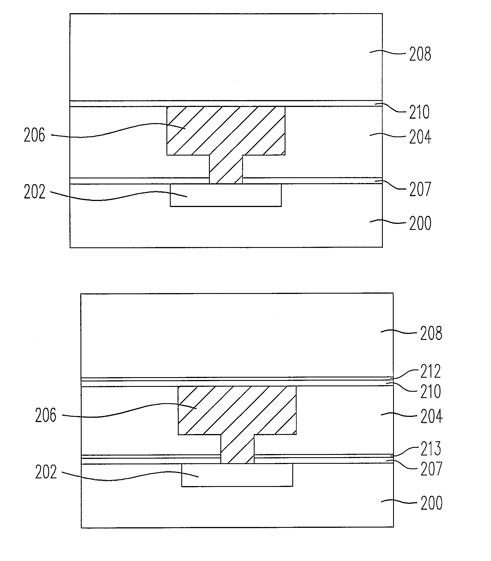
[0024] In the embodiments of this invention, the substrate excluding the conductive part also includes a porous low-k material and requires a UV-absorption layer for protection. Such a substrate may be an IMD layer in which an interconnect structure has been formed. However, the substrate is not restricted to be a porous low-k material layer, but can be any film with a conductive part thereon.

[0025]FIGS. 2A-2E illustrate five interconnect structures in a cross-sectional view according to different embodiments of this invention. Referring to FIG. 2A first, the substrate 200 has a conductive part 202 thereon, which may be a conductive line. A porous low-k layer 204 is disposed on the substrate 200. A damascene structure 206 like a dual-damascene structure is disposed in the porous low-k layer 204 electrically connecting with the conductive part 202, wherein the damascene structure 206 may include metal. A UV-absorption layer 207 is disposed between the substrate 200 and the porous lo...


PUM

PropertyMeasurementUnit
dielectric constantaaaaaaaaaa
dimensionaaaaaaaaaa
parasitic capacitanceaaaaaaaaaa

Abstract

A method for fabricating an interconnect structure is described. A substrate with a conductive part thereon is provided, a first porous low-k layer is formed on the substrate, and then a first UV-curing step is conducted. A damascene structure is formed in the first porous low-k layer to electrically connect with the conductive part, and then a first UV-absorption layer is formed on the first porous low-k layer and the damascene structure. A second porous low-k layer is formed on the first UV-absorption layer, and a second UV-curing step is conducted.

Description

CROSS-REFERENCE TO RELATED APPLICATION [0001] This is a divisional application of patent application Ser. No.11 / 163, 285, filed on Oct. 13, 2005. The entirety of the above-mentioned patent application is hereby incorporated by reference herein and made a part of this specification.BACKGROUND OF THE INVENTION [0002] 1. Field of the Invention [0003] The present invention relates to a method of fabricating an integrated circuit structure. More particularly, the present invention relates to a method of fabricating an interconnect structure. [0004] 2. Description of the Related Art [0005] With the rapid reduction in dimension of IC device, the line pitch of interconnect is decreased unceasingly. Because the RC delay effect gets more significant at reduced line pitch, SiO2 with a dielectric constant near 4.0 cannot be used as an IMD material in the interconnect structure. Therefore, low-k materials are widely used instead of SiO2 to reduce the parasitic capacitance, so as to inhibit the R...

Claims


Application Information

Patent Timeline
Patent Type & Authority Applications(United States)
IPC IPC(8): C08F2/46H01L21/4763C08J7/18
CPCH01L21/7682H01L21/76829H01L21/76832H01L21/76834H01L23/5329H01L23/53295H01L2924/0002H01L2221/1047H01L2924/00
Inventor HSU, FENG-YULIU, CHIH-CHIENHUANG, JIM-JEYCHEN, JEI-MING
Owner UNITED MICROELECTRONICS CORP
Why Eureka
Try Eureka