Interconnect structure and fabricating method thereof

Active Publication Date: 2007-04-19
UNITED MICROELECTRONICS CORP
View PDF4 Cites 5 Cited by
  • Summary
  • Abstract
  • Description
  • Claims
  • Application Information

AI Technical Summary

Benefits of technology

[0008] In view of the foregoing, this invention provides an interconnect structure to

Problems solved by technology

With the rapid reduction in dimension of IC device, the line pitch of interconnect is decreased unceasingly.
Therefore, a lower porous low-k layer is cured more times and receives more UV-irradiation than an upper one, so that the phys

Method used


Image

  • Interconnect structure and fabricating method thereof
  • Interconnect structure and fabricating method thereof
  • Interconnect structure and fabricating method thereof

Examples


Example

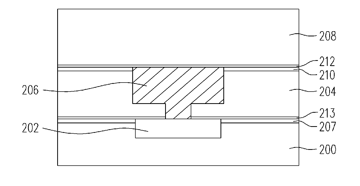
[0025] In the embodiments of this invention, the substrate excluding the conductive part also includes a porous low-k material and requires a UV cutting layer for protection. Such a substrate may be an IMD layer in which an interconnect structure has been formed. However, the substrate is not restricted to be a porous low-k material layer, but can be any film with a conductive part thereon.

[0026] It is particularly noted that in this invention, a UV reflection layer means a layer effective in UV reflection only, such as, a UV-SiN layer. A UV absorption layer means a layer effective in UV absorption only, such as, a SiON layer. A UV reflection-absorption layer means a layer that is effective in both reflection and absorption. The reflectivity of a UV reflection or reflection-absorption layer may be up to 0.5 or higher.

[0027]FIGS. 2A-2E illustrate five interconnect structures in a cross-sectional view according to different embodiments of this invention. Referring to FIG. 2A first, ...


PUM


Abstract

An interconnect structure is described, disposed on a substrate with a conductive part thereon and including a first porous low-k layer on the substrate, a damascene structure in the first porous low-k layer electrically connecting with the conductive part, a second porous low-k layer over the first porous low-k layer and the damascene structure, and a UV cutting layer at least between the first and the second porous low-k layers, wherein the UV cutting layer is a UV reflection layer or a UV reflection-absorption layer.

Description

CROSS-REFERENCE TO RELATED APPLICATION [0001] This application is a continuation-in-part of a prior application of U.S. patent application Ser. No. 11 / 163,285 filed on Oct. 13, 2005. All disclosures are incorporated herewith by reference.BACKGROUND OF THE INVENTION [0002] 1. Field of the Invention [0003] The present invention relates to an integrated circuit structure and fabrication thereof. More particularly, the present invention relates to an interconnect structure and a method for fabricating the same. [0004] 2. Description of the Related Art [0005] With the rapid reduction in dimension of IC device, the line pitch of interconnect is decreased unceasingly. Because the RC delay effect gets more significant at reduced line pitch, SiO2 with a dielectric constant near 4.0 cannot be used as an IMD material in the interconnect structure. Therefore, low-k materials are widely used instead of SiO2 to reduce the parasitic capacitance, so as to inhibit the RC delay effect and the cross-t...

Claims


Application Information

Patent Timeline
IPC IPC(8): H01L23/52
CPCH01L21/76834H01L23/5329H01L23/53295H01L21/7682H01L21/76829H01L21/76832H01L2221/1047H01L2924/0002H01L2924/00
Inventor HSU, FENG-YULIU, CHIH-CHIENHUANG, CHUN-CHIEHCHEN, JEI-MINGSUNG, SHU-JEN
Owner UNITED MICROELECTRONICS CORP
Why Eureka
Try Eureka