In-plane switching mode liquid crystal display device, and method for manufacturing the same

a liquid crystal display and switching mode technology, applied in non-linear optics, instruments, optics, etc., can solve the problems of increasing luminance, deteriorating alignment of liquid crystals, and not allowing light transmission, so as to improve black luminance

Inactive Publication Date: 2007-05-03
LG DISPLAY CO LTD
View PDF9 Cites 3 Cited by
  • Summary
  • Abstract
  • Description
  • Claims
  • Application Information

AI Technical Summary

Benefits of technology

[0020] An advantage of the present invention is to provide an in-plane switching mode liquid crystal display device and a method for manufacturing the same, in which a vertical alignment film is employed to prevent light leakage at an edge of an electrode that is not well rubbed, thereby improving black luminance.
[0021] Additional features and advantages of the invention will be set forth in the description which follows, and in part will be apparent from the description, or may be learned by practice of the invention. These and other advantages of the invention will be realized and attained by the structure particularly pointed out in the written description and claims hereof as well as the appended drawings.
[0022] To achieve these and other advantages and in accordance with the purpose of the present invention, as embodied and broadly described, there is provided an in-plane switching mode liquid crystal display device comprising a thin film transistor array substrate, a color filter substrate, and a liquid crystal. The thin film transistor array substrate has a common electrode and a pixel electrode arranged in an alternating pattern with each other, and has a first alignment film provided on the common electrode and the pixel electrode so as to align liquid crystal molecules in a vertical direction. The color filter substrate faces the thin film transistor array substrate, and has a second alignment film for aligning the liquid crystal molecules in a vertical direction. Liquid crystal is injected between the thin film transistor array substrate and the color filter substrate.
[0023] In another aspect of the present invention, there is provided a method for manufacturing an in-plane switching mode liquid crystal display device, comprising: providing a common electrode and a pixel electrode on an pixel region wherein the common and pixel electrodes are not in a switching region of a pixel region, depositing a metal thin film on the pixel region, rubbing the metal thin film, and anodizing the rubbed metal thin film to provide an inorganic vertical alignment film.
[0024] In a further another aspect of the present invention, there is provided a method for manufacturing an in-plane switching mode liquid crystal display device, comprising a common electrode and a pixel electrode on an pixel region wherein the common and pixel electrodes are not in a switching region of a pixel region, depositing an organic vertical alignment film on the pixel region, and rubbing the organic vertical alignment film.

Problems solved by technology

An in-plane switching mode liquid crystal display device according to the related art is in a normally black state, and does not allow light transmission before voltage is applied.
However, if the horizontal alignment film is used in the in-plane switching mode, rubbing is not performed due to an electrode edge part at a side of a rubbing direction.
As such, in the horizontal alignment film, if the rubbing is not performed, the alignment of the liquid crystal is remarkably deteriorated and, for example, there is a drawback in that, when black is embodied, the region generates phase delay due to non-uniform rubbing and therefore, light leakage is caused and luminance is increased, thereby not clearly embodying the black.

Method used


Image

  • In-plane switching mode liquid crystal display device, and method for manufacturing the same
  • In-plane switching mode liquid crystal display device, and method for manufacturing the same
  • In-plane switching mode liquid crystal display device, and method for manufacturing the same

Examples


Embodiment Construction

[0035] Reference will now be made in detail to embodiments of the present invention, examples of which are illustrated in the accompanying drawings.

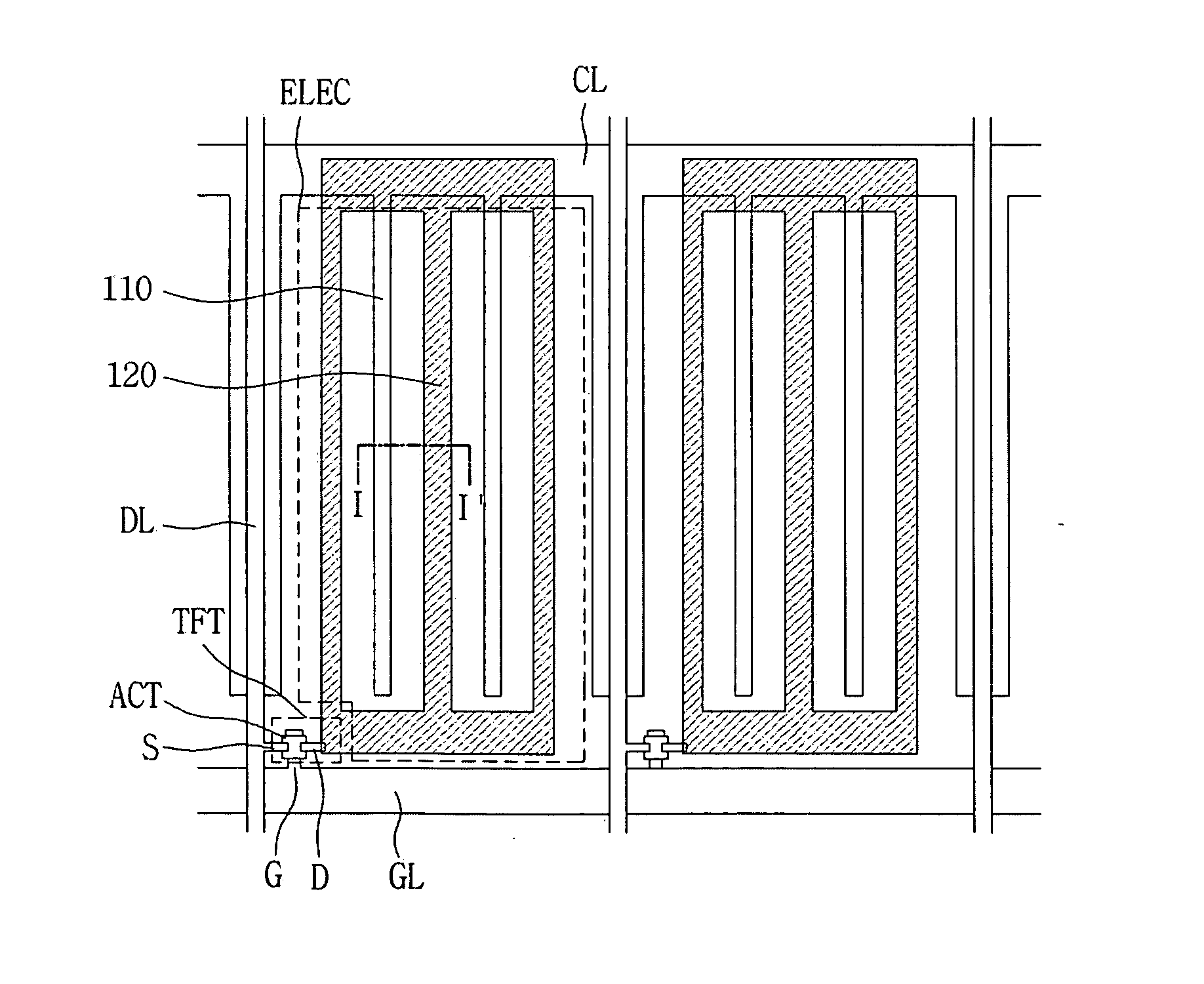
[0036]FIG. 3 is a plan view illustrating an in-plane switching mode liquid crystal display device according to an embodiment of the present invention.

[0037] In FIG. 3, the in-plane switching mode liquid crystal display device according to an embodiment of the present invention, a gate line (GL) and a data line (DL) are arranged and cross with each other to define a pixel region. The pixel region is divided into a switching region (TFT) in which a thin film transistor is positioned, and an pixel region (ELEC) other than the switching region (TFT).

[0038] In a detailed description, the gate line (GL) and a common line (CL) are arranged in parallel in a first direction, and the data line (DL) crossing the gate line (GL) is arranged in a second direction. A gate electrode (G), a semiconductor layer (ACT) provided thereon, and a source elec...


PUM

PropertyMeasurementUnit
pretilt angleaaaaaaaaaa
angleaaaaaaaaaa
rubbing depthaaaaaaaaaa

Abstract

Provided are an in-plane switching mode liquid crystal display device and a method for manufacturing the same. The device comprises a thin film transistor array substrate, a color filter substrate, and a liquid crystal. The thin film transistor array substrate has a common electrode and a pixel electrode arranged in an alternating pattern with each other, and has a first alignment film provided on the common electrode and the pixel electrode so as to align liquid crystal molecules in a vertical direction. The color filter substrate faces the thin film transistor array substrate, and has a second alignment film that aligns the liquid crystal molecules in a vertical direction. Liquid crystal is injected between the thin film transistor array substrate and the color filter substrate.

Description

[0001] This application claims the benefit of Korean Patent Application No. 2005-0104057, filed on Nov. 02, 2005, which is hereby incorporated by reference for all purposes as if fully set forth herein. BACKGROUND OF THE INVENTION [0002] 1. Field of the Invention [0003] The present invention relates to a liquid crystal display device, and more particularly, to an in-plane switching mode liquid crystal display device and a method for manufacturing the same. [0004] 2. Discussion of the Related Art [0005] A liquid crystal display device refers to a display apparatus in which a liquid crystal material having anisotropic permittivity is provided between a color filter (CF) substrate and a thin film transistor (TFT) array substrate that are upper and lower transparent insulating substrates. An intensity of an electric field provided in the liquid crystal material is controlled such that a molecular arrangement of the liquid crystal material is changed, and an amount of light transmitted t...

Claims


Application Information

Patent Timeline
Patent Type & Authority Applications(United States)
IPC IPC(8): G02F1/1343
CPCG02F1/133784G02F1/134363G02F2001/133742G02F1/133742G02F1/1337
Inventor LIM, YOUNG NAM
Owner LG DISPLAY CO LTD
Why Eureka
Try Eureka