Display apparatus

a display apparatus and active matrix technology, applied in the field of active matrix display apparatus, can solve the problem that the display quality cannot be improved, and achieve the effect of reducing the number of slits of the counter electrode, expanding the display area, and eliminating luminance variations

Inactive Publication Date: 2008-07-03
INTELLECTUAL KEYSTONE TECH LLC
View PDF74 Cites 66 Cited by
  • Summary
  • Abstract
  • Description
  • Claims
  • Application Information

AI Technical Summary

Benefits of technology

[0010]Specifically, in the present invention, since a data line, a group of pixels connected thereto, one common power-feed line, a group of pixels connected thereto, and a data line for supplying a pixel signal to the group of pixels are assumed to be one unit and this is repeated in the extension direction of scanning lines, pixels for two rows are driven by one common power-feed line. Therefore, the formation area of common power-feed lines can be made more narrow than in a case in which a common power-feed line is formed for each group of pixels for one row, the light-emission area of the pixels can be expanded correspondingly. Therefore, it is possible to improve display performance, such as luminance, contrast ratio, and so on.
[0018]For example, the construction is formed in such a way that the polarity of the driving. current in each pixel is the same in the extension direction of the data lines and that, in the extension direction of the scanning lines, the polarity of the driving current in each pixel is inverted for each pixel or every two pixels. The construction may also be formed in such a way that the polarity of the driving current in each pixel is the same in the extension direction of the scanning lines and that, in the extension direction of the data lines, the polarity of the driving current in each pixel is inverted for each pixel or every two pixels. Of these constructions, in the case of the construction in which the polarity of the driving current is inverted every two pixels, for the pixels through which driving current of the same polarity flows, a counter electrode can be used in common between adjacent pixels, making it possible to reduce the number of slits of the counter electrode. That is, polarity inversion can be realized without increasing the resistance value of the counter electrodes through which a large current flows.

Problems solved by technology

However, in comparison with the liquid-crystal display apparatus, in the display apparatus 1A, there is a problem in that the display quality cannot be improved because the pixels 7 are narrower by an amount corresponding to the requirement of the second TFT 30 and the common power-feed lines “com”.

Method used


Image

  • Display apparatus
  • Display apparatus
  • Display apparatus

Examples


first embodiment

(Overall Construction of Active-Matrix Substrate)

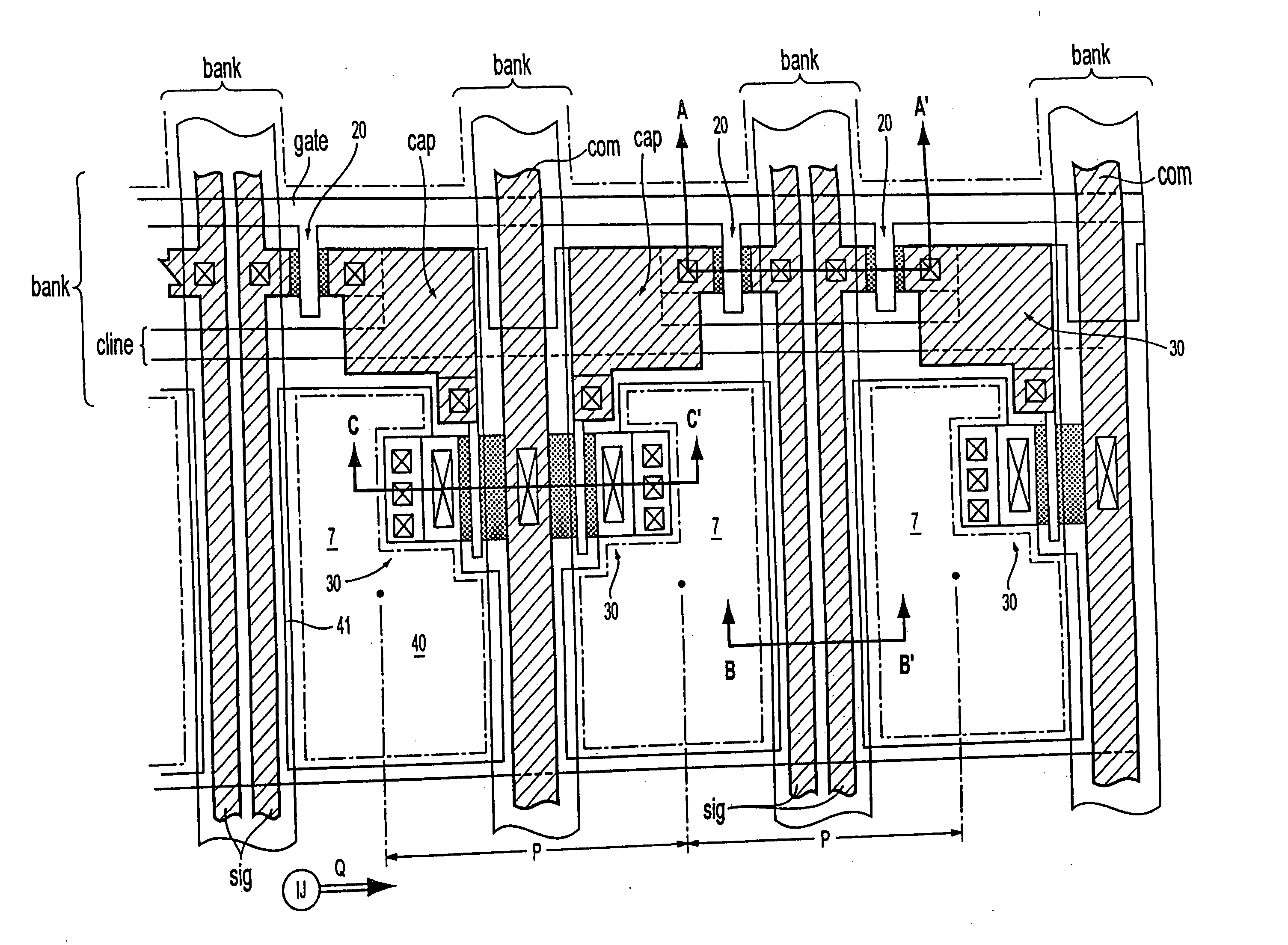
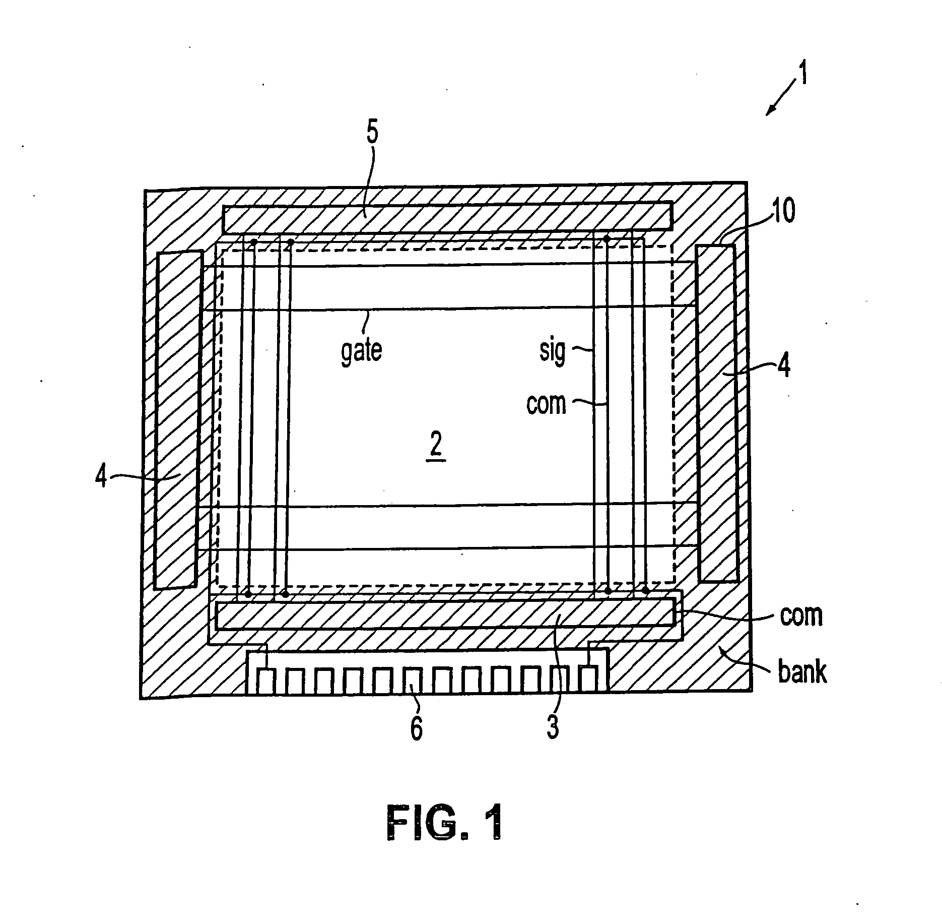
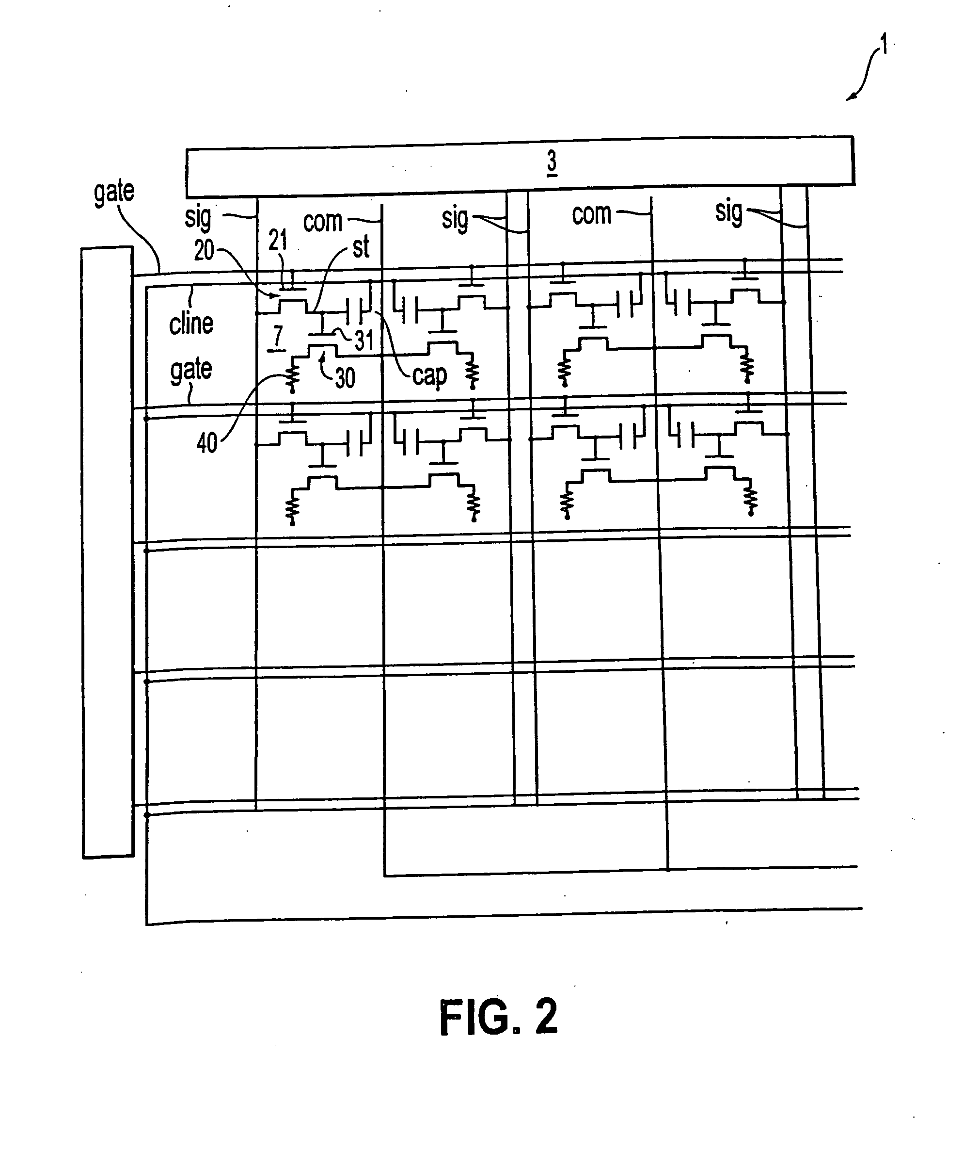
[0075]FIG. 1 is a block diagram schematically showing the overall layout of a display apparatus. FIG. 2 is an equivalent circuit diagram of an active matrix formed therein.

[0076]As shown in FIG. 1, in a display apparatus 1 of this embodiment, the central portion of a transparent substrate 10, which is a base body thereof, is formed into a display section 2. On both ends of the data lines “sig” of the peripheral portion of the transparent substrate 10, a data-side driving circuit 3 for outputting an image signal, and a checking circuit 5 are formed, and on both ends of the scanning lines “gate”, a scanning-side driving circuit 4 for outputting a scanning signal is formed. In these driving circuits 3 and 4, a complementary TFT is formed by an n_type TFT and a p_type TFT. This complementary TFT forms a shift register, a level shifter, an analog switch, etc. On the transparent substrate 10, a mounting pad 6, which is a group of terminals ...

second embodiment

[0117]Although in the above-described first embodiment, the construction is formed in such a way that the light-emission elements 40 are driven by driving current of the same polarity in any pixel 7, as will be described below, the construction may be formed in such a way that the same number of two types of pixels 7, in which the light-emission elements 40 are driven by a driving current whose polarity is inverted, are among a plurality of pixels 7 to which driving current is passed in a section between the pixels and the same common power-feed line “com”.

[0118]Examples of such constructions are described with reference to FIGS. 13 to 17. FIG. 13 is a block diagram of an embodiment in which two types of pixels, in which the light-emission elements 40 are driven by a driving current whose polarity is inverted, are structured. FIGS. 14 and 15 are each an illustration of a scanning signal, an image signal, the potential of common power-feed lines, and a potential of a potential holdin...

third embodiment

[0127]From the viewpoint of the fact that pixels are arranged in such a way that driving current flows at an opposite polarity in a section between the pixels and the same common power-feed line “com”, each pixel may be arranged as shown in FIG. 18. In this embodiment, since the construction of each of the pixels 7A and 7B is similar to that of the second embodiment. Therefore, the description has been omitted. In FIG. 18 and FIGS. 19 to 21, for describing each embodiment to be described below, a pixel corresponding to the pixel 7A described with reference to FIGS. 13, 14, and 16 is shown by the sign (−), and a pixel corresponding to the pixel 7B described with reference to FIGS. 13, 15, and 16 is shown by the sign (+).

[0128]As shown in FIG. 18, in this embodiment, the construction is formed in such a way that the polarity of the driving current in each of the pixels 7A and 7B is the same along the extension direction of the data lines “sigA” and “sigB” and that along the extension ...


PUM


Abstract

For the purpose of providing a display apparatus capable of improving display quality by expanding the light-emission area of pixels by improving the layout of pixels and common power-feed lines formed on a substrate, pixels (7A, 7B) including a light-emission element (40), such as an electroluminescence element or an LED element, are arranged on both sides of common power-feed lines (com) so that the number of common power-feed lines (com) is reduced. Further, the polarity of a driving current flowing between the pixels (7A, 7B) and the light-emission element (40) is inverted so that the amount of current flowing through the common power-supply lines “com” is reduced.

Description

[0001]This is a Continuation of application Ser. No. 10 / 968,984, filed Oct. 21, 2004, which is a Divisional of application Ser. No. 10 / 367,849 filed Feb. 19, 2003, which is a Continuation of application Ser. No. 09 / 242,904, which is now U.S. Pat. No. 6,618,029, which is the U.S. National Stage of PCT / JP98 / 02982, filed Jul. 1, 1998, which claims priority to Japanese Application No. 9-177455, which was filed Jul. 2, 1997. The entire disclosures of the prior applications are hereby incorporated by reference herein in their entireties.TECHNICAL FIELD[0002]The present invention relates to an active-matrix-type display apparatus which uses light-emission elements, such as EL (electroluminescence) elements that emit light when driving current flows through an organic semiconductor film or LED (light-emitting diode) elements, and thin-film transistors (hereinafter referred to as “TFTs”) that control the light-emission operation of this light-emission element. More particularly, the present ...

Claims


Application Information

Patent Timeline
Patent Type & Authority Applications(United States)
IPC IPC(8): G06F3/038G09G3/30H05B33/12G09F9/30G09G3/20H01L27/32H01L51/50H05B33/14H05B33/26
CPCG09G3/30H01L27/124G09G3/3233G09G2300/0426G09G2300/0465G09G2300/0809G09G2310/0254G09G2320/0209G09G2330/021H01L27/3223H01L27/3244H01L27/3246H01L27/3265H01L27/3276G09G3/32H10K59/88H10K59/122H10K59/12H10K59/1216H10K59/131G09F9/30
Inventor OZAWA, TOKUROH
Owner INTELLECTUAL KEYSTONE TECH LLC
Why Eureka
Try Eureka