Method for checking the pattern density of a semiconductor chip design with variable checking box size and variable stepping distance

a chip design and pattern density technology, applied in the field of semiconductor wafer design and manufacturing, can solve the problems of increasing the number of manufacturing errors, increasing the difficulty and constraining of larger process windows, and reducing the number of checking boxes. the effect of reducing the size of the checking box

Inactive Publication Date: 2007-05-03
IBM CORP
View PDF10 Cites 6 Cited by
  • Summary
  • Abstract
  • Description
  • Claims
  • Application Information

AI Technical Summary

Benefits of technology

[0009] It is another object to provide a method for hierarchically reducing the checking box size, discarding areas that are guarantied to pass, and then fracturing questionable areas into smaller checking areas.

Problems solved by technology

As the CMOS technology evolves and moves towards the 90 nm generation and beyond, fabrication costs associated thereof play an ever increasing role.
In the aforementioned sub-micron technologies, larger process windows and uniform manufacturing is becoming increasingly more difficult and constraining, particularly, on the physical layouts and their ensuing verification requirements.
The problem is particularly acute when attempts are made to control manufacturing variations related to Chemical Mechanical Polish (CMP) which requires evenly distributed patterns on layers that make up the fabricated semiconductor wafer.
One problem with this approach is that large areas where no patterns exist are checked with the same, small-sized checking box.
However, a mid-sized checking box and step size creates a two-dimensional sampling problem which makes the results of the check dependent on the relative location of shapes and patterns in the design.
As a result, errors that exist at one level of hierarchy may not be reported until the origin of the design shifts at a higher level of the hierarchical layout, thereby shifting the edges of the checking boxes.
Although this technique is advantageous in its use of different checking box sizing and its ability of providing efficient positioning algorithms to perform density checks, it is hampered by its limitation of consistently dividing the checking box side by 2, and is further stymied by its inability to skip forward when the density is very high.

Method used


Image

  • Method for checking the pattern density of a semiconductor chip design with variable checking box size and variable stepping distance
  • Method for checking the pattern density of a semiconductor chip design with variable checking box size and variable stepping distance
  • Method for checking the pattern density of a semiconductor chip design with variable checking box size and variable stepping distance

Examples


Embodiment Construction

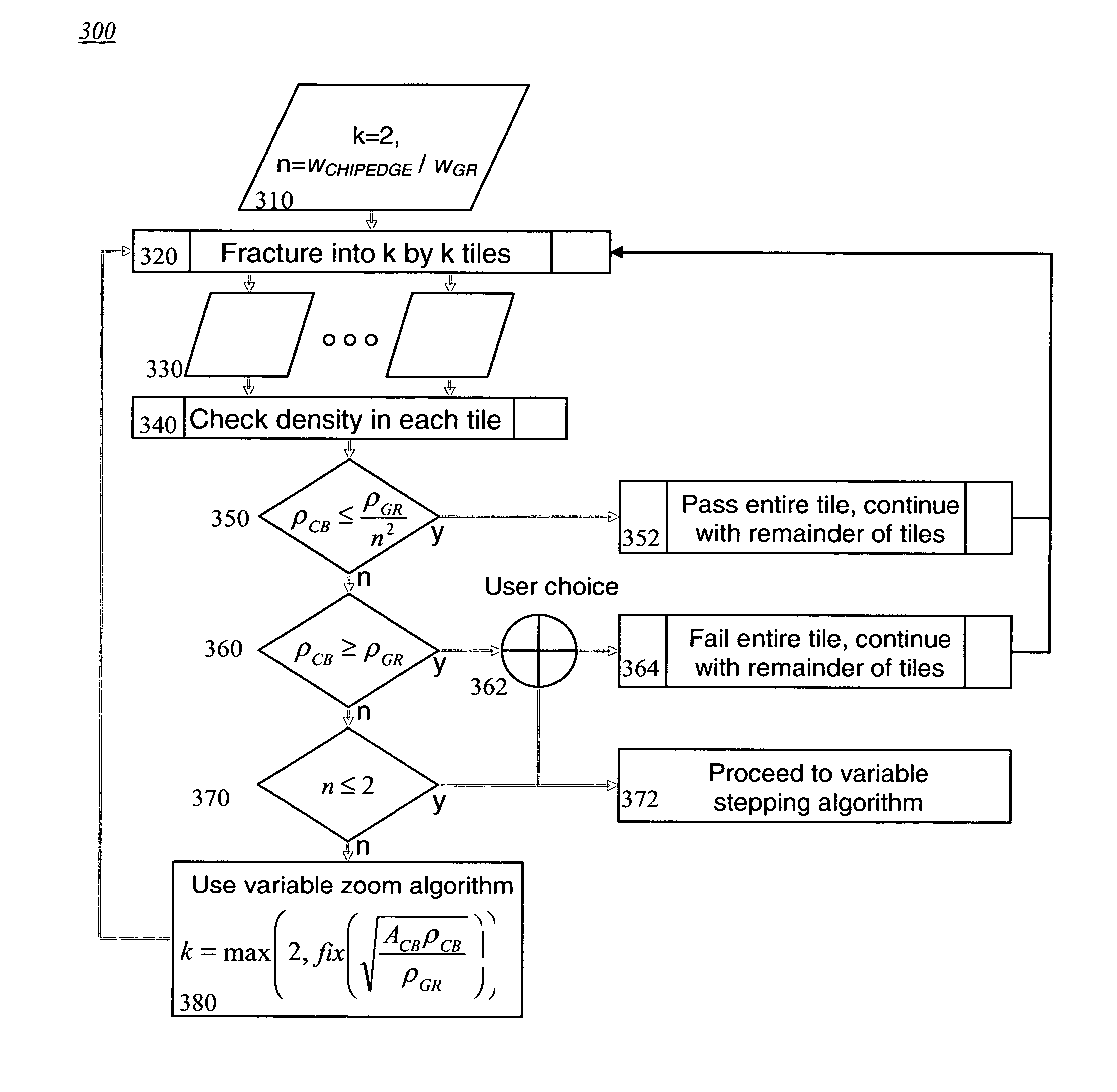
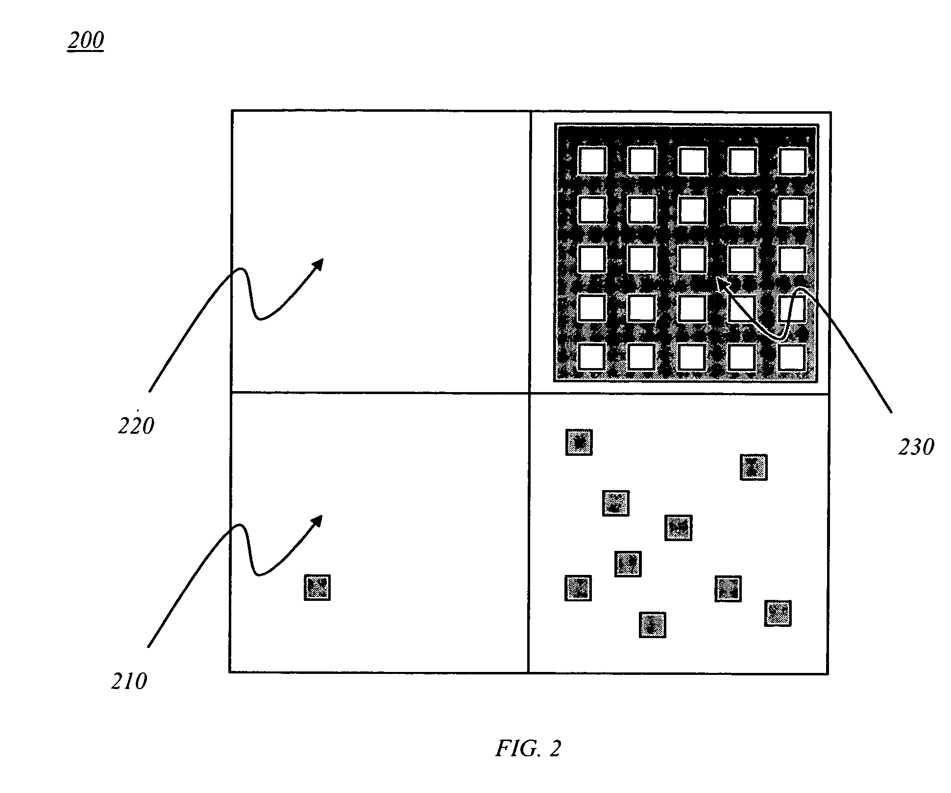
[0031] For the purposes of the present description, there will be a focus on a groundrule mandated local pattern density maximum. The same concepts may also be applied to a pattern density minimum by one skilled in the art.

[0032] Local pattern density is defined as the amount of pattern within a checking box of a size specified by the same groundrule. For example, a groundrule may specify that the maximum pattern density in a chip is 50% within a checking box of 20 μm per edge. In this example, a design in which a 20 μm×20 μm box can be placed and contain more than 200 μm2 of pattern is considered to fail because the density of pattern is greater than 50%.

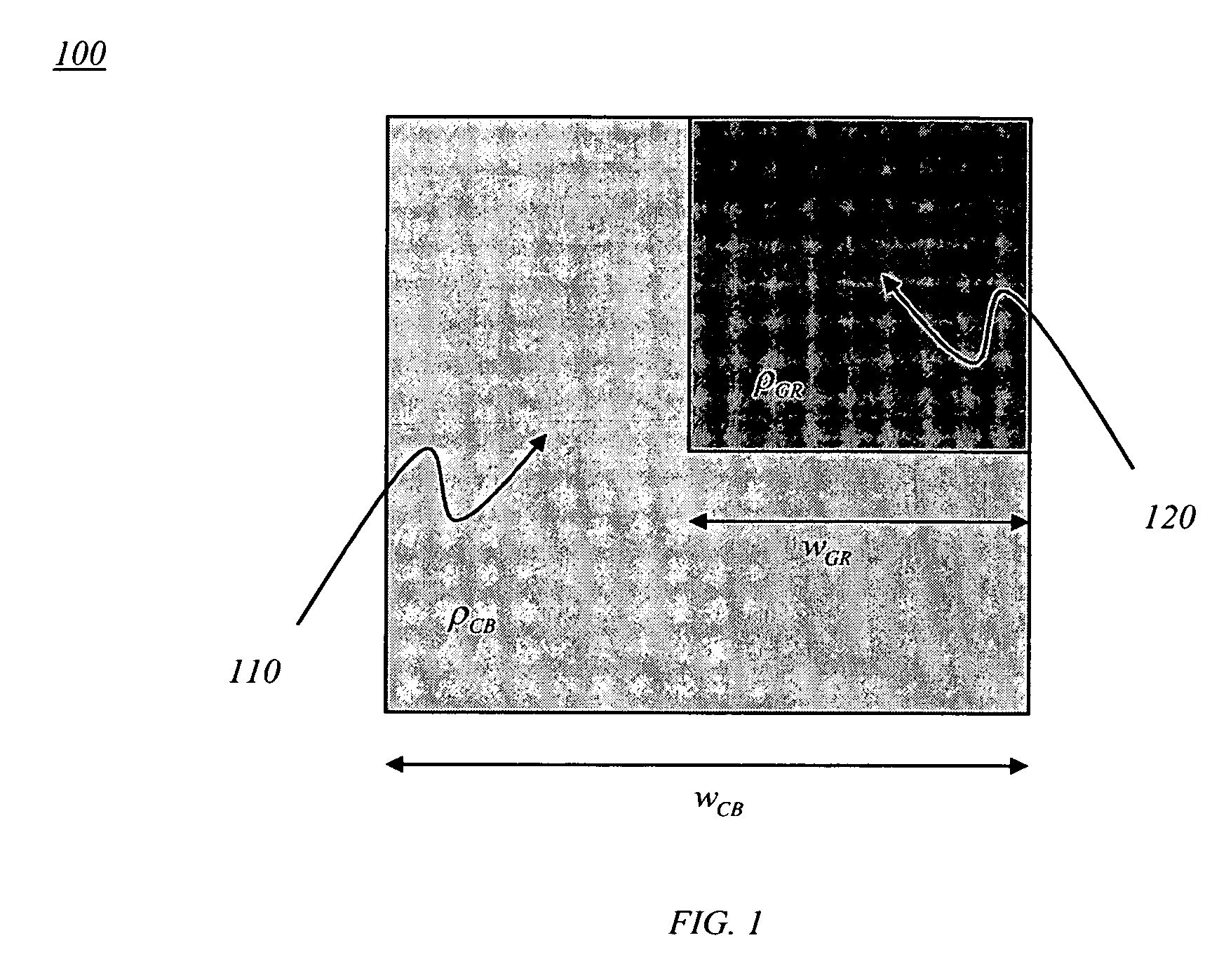
[0033] The inventive method requires that the area of the pattern density of the entire chip must be found. Based on the pattern density one can pass the entire chip, fail the entire chip, or decide that it must be analyzed in smaller areas. This will become more understandable when looking at extreme cases. If the entire design ...


PUM


Abstract

A method for checking the pattern density of a chip layout is described. Initially, the design area is subdivided into a plurality of large checking boxes. Large portions of the chip are discarded from further checking if they are found to fall within acceptable limits at the more stringent and scaled box size. The box size is successively reduced using an appropriate density for each box size until key problem areas are identified on the chip. After the check of a non-failing area, the reduction in checking box size is determined by the detected pattern density. Once the checking box size approximates that of the checking box size as dictated by the groundrule, the checking box size is fixed to that of the groundrule. Rather than using steps that are of the order of the width of the checking box, the box is stepped in an adaptive manner where the distance stepped is relative to the measured pattern density to guarantee that all the errors are captured and reported, regardless of their location from the origin.

Description

BACKGROUND OF THE INVENTION [0001] This invention relates to the design and manufacture of semiconductor wafers and more particularly to a method for checking the pattern density of a chip design layout. [0002] As the CMOS technology evolves and moves towards the 90 nm generation and beyond, fabrication costs associated thereof play an ever increasing role. In order to maximize the yield, process engineers must achieve a consistent predictability and uniformity of the manufactured devices, contact shapes, channel lengths, interlayer dielectrics, and the like. [0003] In the aforementioned sub-micron technologies, larger process windows and uniform manufacturing is becoming increasingly more difficult and constraining, particularly, on the physical layouts and their ensuing verification requirements. [0004] The problem is particularly acute when attempts are made to control manufacturing variations related to Chemical Mechanical Polish (CMP) which requires evenly distributed patterns ...

Claims


Application Information

Patent Timeline
Patent Type & Authority Applications(United States)
IPC IPC(8): G06K9/00
CPCG06F17/5081G06F2217/12G06F30/398G06F2119/18Y02P90/02
Inventor SANDERSON, DAVID I.SCHNABEL, CHRISTOPHER M.
Owner IBM CORP
Why Eureka
Try Eureka