Method of forming solder mask and wiring board with solder mask

a technology of solder mask and wiring board, which is applied in the field of forming a solder mask on a wiring board, can solve the problems of increasing production cost, slowing down the fabrication process, and increasing production cost, and achieve the effect of reducing the time needed for fabricating solder

Active Publication Date: 2007-05-03
UNIMICRON TECH CORP
View PDF3 Cites 7 Cited by
  • Summary
  • Abstract
  • Description
  • Claims
  • Application Information

AI Technical Summary

Benefits of technology

[0011] An objective of the present invention is to provide a method of forming a solder mask capable of reducing the time needed to fabricate the solder mask on a high wiring density wiring board.
[0012] Another objective of the present invention is to provide a high wiring density wiring board having a solder mask that shortens the fabrication time.
[0020] In brief, the present invention utilizes a screen-printing or photolithographic process together with an ink-jet printing process to fabricate a solder mask on a wiring board with a shorter production time and a higher alignment precision and reliability. Hence, the method is suitable for mass-producing wiring boards with a high wiring density so that the productivity is increased and the production cost is reduced.

Problems solved by technology

However, the aforesaid method not only complicate the process of forming the solder mask 130, but also considerably increases the production cost.
Although an ink-jet printing process can compensate for the expansion and contraction to produce a highly aligned solder mask 130 with a relatively small gap d1, the need for coating a large wiring board 100 often leads to a slowdown of the fabrication process.
Consequently, the increase of production cost makes the ink-jet printing technique not suitable for mass-producing wiring boards 100 with high wiring density.

Method used


Image

  • Method of forming solder mask and wiring board with solder mask
  • Method of forming solder mask and wiring board with solder mask
  • Method of forming solder mask and wiring board with solder mask

Examples


first embodiment

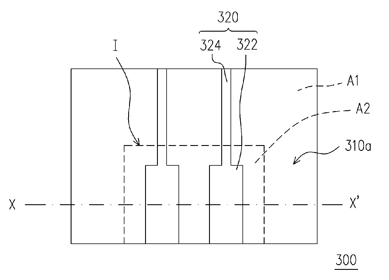
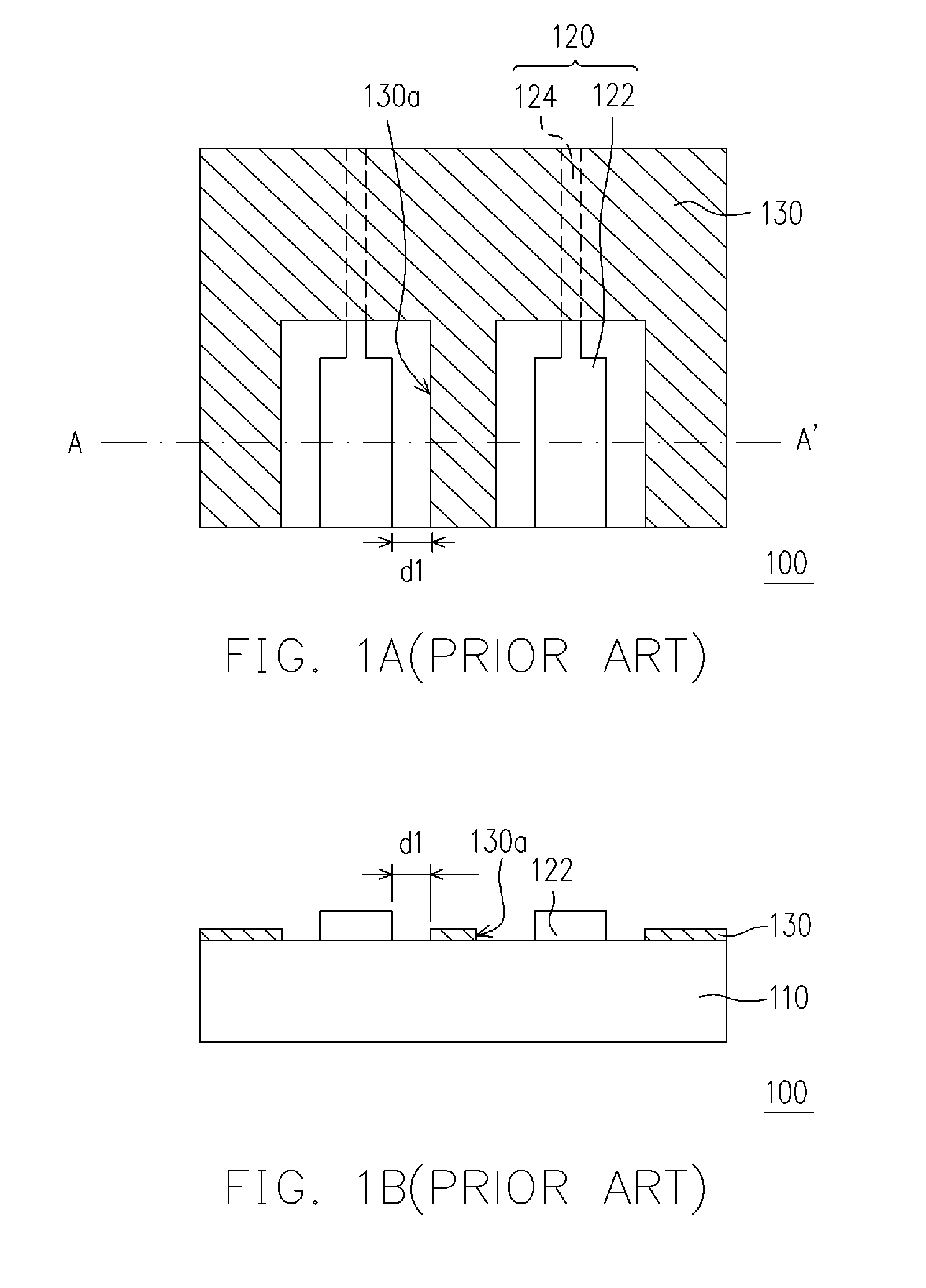
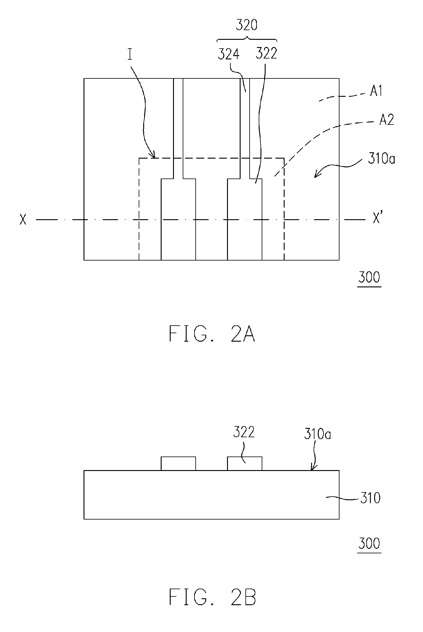
[0037] In the following, an embodiment is described to illustrate the process of forming a solder mask over a wiring board. FIGS. 2A, 3A and 4A are top views showing a method of forming a solder mask according to a first embodiment of the present invention. FIG. 2B is a cross-sectional view along line X-X′ of FIG. 2A. FIG. 3B is a cross-sectional view along line X-X′ of FIG. 3A. FIG. 4B is a cross-sectional view along line X-X′ of FIG. 4A. In FIGS. 2A and 2B, the wiring board 300 includes a base layer 310 and a wiring pattern 320 disposed on a surface 310a of the base layer 310. The base layer 310 is, for example, a single insulating layer or comprises a plurality of patterned conductive layers and at least an insulation layer alternately stacked over each other. The wiring pattern 320 includes a plurality of pads 322 and a plurality of conductive traces 324. The pads 322 are used for supporting and providing a means of conduction with external electronic devices and the conductive ...

second embodiment

[0043] In the following, another embodiment is used to explain the process of forming a solder mask over a wiring board. FIGS. 6A, 7A, 8A and 9A are top views showing a method of forming a sub solder mask according to a second embodiment of the present invention. FIG. 6B is a cross-sectional view along line Y-Y′ of FIG. 6A. FIG. 7B is a cross-sectional view along line Y-Y′ of FIG. 7A. FIG. 8B is a cross-sectional view along line Y-Y′ of FIG. 8A. FIG. 9B is a cross-sectional view along line Y-Y′ of FIG. 9A. As shown in FIGS. 6A and 6B, the wiring board 400 has a structure similar to the wiring board 300 in FIG. 2A. The wiring board 400 includes a base layer 410 and a wiring pattern 420 disposed on the surface 410a of the base layer 410. Since the process of patterning the base layer 410 is identical to the process used in the first embodiment, a detailed description is omitted. The wiring pattern 420 includes a plurality of pads 422 and a plurality of conductive traces 424. In the se...


PUM

PropertyMeasurementUnit
wiring densityaaaaaaaaaa
thicknessaaaaaaaaaa
currentsaaaaaaaaaa

Abstract

A method of forming solder mask, suitable for forming a solder mask on the surface of a wiring board, is provided. The surface of the wiring board includes a first region and a second region, and the surface of the wiring board has a wiring pattern thereon. The method includes forming a first sub solder mask in the first region on the surface of the wiring board by performing a screen-printing or a photolithographic process, and forming a second sub solder mask in the second region on the surface of the wiring board by performing an ink-jet printing process. The method not only improves the precision of the solder mask alignment on the wiring board and its reliability, but also increases the production rate and lowers the manufacturing cost.

Description

CROSS-REFERENCE TO RELATED APPLICATION [0001] This application claims the priority benefit of Taiwan application serial no. 94138042, filed on Oct. 31, 2005. All disclosure of the Taiwan application is incorporated herein by reference. BACKGROUND OF THE INVENTION [0002] 1. Field of the Invention [0003] The present invention relates to a method of forming a solder mask. More particularly, the present invention relates to a method of forming a solder mask on a wiring board. [0004] 2. Description of the Related Art [0005] With the rapid development of digital electronic technologies, printed wiring boards are found widely used in digital electronic products. Electronic products, such as mobile phones, computers, and digital cameras etc., are fabricated with a printed wiring board. In other words, wiring boards are used for almost all of the electronic devices. According to the fabricating method, wiring boards can be divided into two major types: a lamination method and a build-up meth...

Claims


Application Information

Patent Timeline
Patent Type & Authority Applications(United States)
IPC IPC(8): G03C5/00
CPCH05K3/28H05K3/3452H05K2203/013H05K2203/0557H05K2203/058H05K2203/1476
Inventor TSENG, TZYY-JANGYU, CHENG-PO
Owner UNIMICRON TECH CORP
Why Eureka
Try Eureka