Vertical diode doped with antimony to avoid or limit dopant diffusion

a technology of antimony and diodes, applied in the field of antimony, can solve problems such as the tendency of dopants to diffus

Inactive Publication Date: 2007-05-10
SANDISK TECH LLC
View PDF11 Cites 19 Cited by
  • Summary
  • Abstract
  • Description
  • Claims
  • Application Information

AI Technical Summary

Problems solved by technology

Dopants tend to diffuse, however, particularly when undoped silicon is deposited d...

Method used


Image

  • Vertical diode doped with antimony to avoid or limit dopant diffusion
  • Vertical diode doped with antimony to avoid or limit dopant diffusion
  • Vertical diode doped with antimony to avoid or limit dopant diffusion

Examples


example

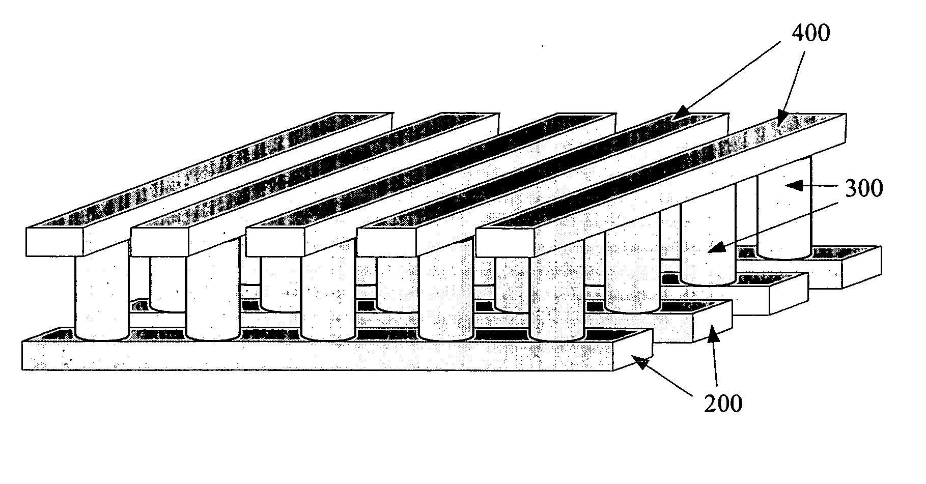
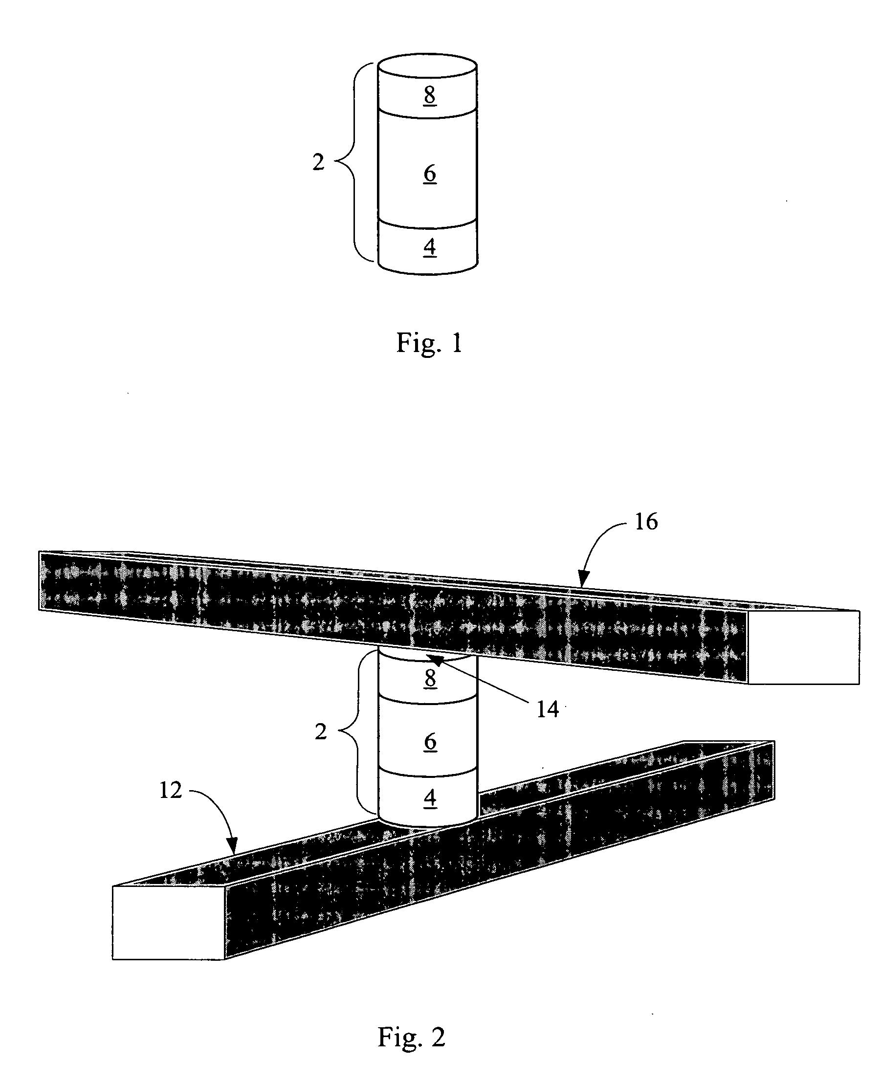
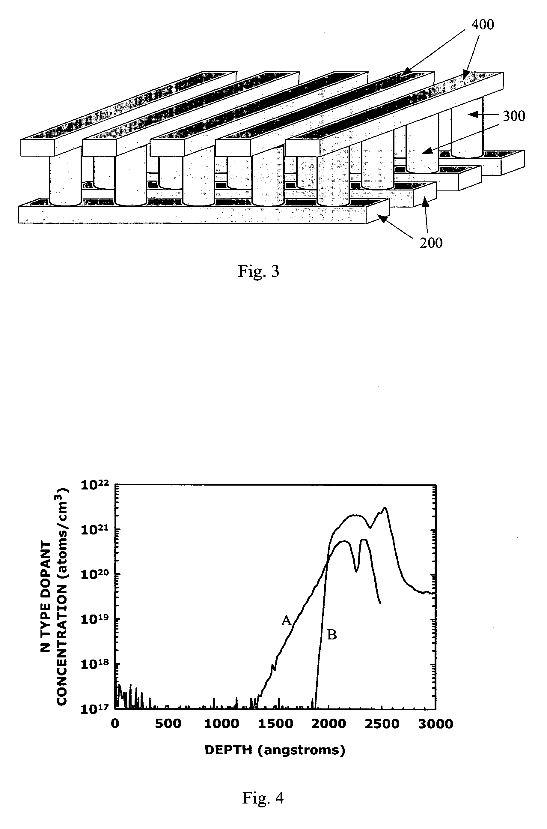
[0033] Fabrication of a single memory level will be described in detail. Additional memory levels can be stacked, each monolithically formed above the one below it.

[0034] Turning to FIG. 5a, formation of the memory begins with a substrate 100. This substrate 100 can be any semiconducting substrate as known in the art, such as monocrystalline silicon, IV-IV compounds like silicon-germanium or silicon-germanium-carbon, III-V compounds, II-VII compounds, epitaxial layers over such substrates, or any other semiconducting material. The substrate may include integrated circuits fabricated therein.

[0035] An insulating layer 102 is formed over substrate 100. The insulating layer 102 can be silicon oxide, silicon nitride, high-dielectric film, Si—C—O—H film, or any other suitable insulating material.

[0036] The first conductors 200 are formed over the substrate and insulator. An adhesion layer 104 may be included between the insulating layer 102 and the conducting layer 106 to help the con...


PUM


Abstract

Use of antimony as an n-type conductivity-enhancing dopant in semiconductor structures having a vertical dopant profile is described. Dopants tend to diffuse, and steep dopant gradients can be difficult to maintain. Specifically, when a silicon layer is doped with phosphorus or arsenic, both n-type dopants, dopant atoms tend to seek the surface as undoped silicon is deposited on top of the n-doped layer, rising through the undoped silicon during deposition. Antimony does not have this tendency, and also diffuses more slowly than either phosphorus or arsenic, and this is advantageously used to dope such structures.

Description

BACKGROUND OF THE INVENTION [0001] The invention relates to use of antimony as a conductivity-enhancing dopant in semiconductor material. [0002] Semiconductor material such as silicon is frequently doped to enhance conductivity. Such dopants may be either p-type or n-type. A device may have an n-type silicon region adjacent to an undoped silicon region, or adjacent to a p-type silicon region. Maintaining these doping distinctions may be crucial to device performance. [0003] Dopants tend to diffuse, however, particularly when undoped silicon is deposited directly on silicon doped with conventional n-type dopants such as phosphorus or arsenic. [0004] There is a need, therefore, to limit dopant diffusion in semiconductor material, particularly in deposited structures with vertically varying dopant profiles. SUMMARY OF THE PREFERRED EMBODIMENTS [0005] The present invention is defined by the following claims, and nothing in this section should be taken as a limitation on those claims. In...

Claims


Application Information

Patent Timeline
IPC IPC(8): H01L31/111
CPCH01L27/1021H01L29/167H01L29/861
Inventor KUMAR, TANMAYHERNER, S. BRAD
Owner SANDISK TECH LLC
Why Eureka
Try Eureka