Display and method for driving display

a display and display technology, applied in the field of display and a display driving method, can solve the problems of non-uniform image quality involving streaks and unevenness, difficult to realize a large-size and high-definition display, and change in the emission luminance of organic el elements, etc., and achieve the effect of uniform image quality

Inactive Publication Date: 2007-05-24
SONY CORP
View PDF7 Cites 55 Cited by
  • Summary
  • Abstract
  • Description
  • Claims
  • Application Information

AI Technical Summary

Benefits of technology

[0036] There is a need for an embodiment of the present invention to provide a display and a method for driving a display that both can realize, with a small number of components, a function to correct variation in the mobility of a drive TFT in addition to a function to compensate a change in the characteristic of an electro-optical element such as an organic EL element and a function to compensate a change (variation from pixel to pixel) in the threshold voltage Vth of the drive TFT for driving the electro-optical element so that a uniform image quality free from streaks and unevenness can be achieved.
[0041] According to embodiments of the invention, two-stage mobility correction is implemented: mobility correction with an intermediate grayscale level is executed in advance, followed by mobility correction with an input signal level. Thus, even if the mobility correction period is constant, mobility correction can be implemented for all the grayscales within the mobility correction period. This feature allows achievement of a uniform image quality free from streaks and unevenness attributed to variation in the mobility from pixel to pixel.

Problems solved by technology

However, a display of the simple-matrix system involves a problem that it is difficult to realize a large-size and high-definition display and other problems although the configuration thereof is simple.
Therefore, age deterioration of the I-V characteristic of the organic EL element leads to a change in the gate-source voltage Vgs of the drive TFT, which results in a change in the emission luminance of the organic EL element.
As is apparent from the aforementioned Equation (1), the difference in the mobility μ of the drive TFT among pixels causes variation in the current Ids flowing through the drive TFT from pixel to pixel, and therefore the emission luminance of the organic EL element varies from pixel to pixel, which results in a nonuniform image quality involving streaks and unevenness.

Method used


Image

  • Display and method for driving display
  • Display and method for driving display
  • Display and method for driving display

Examples


first embodiment

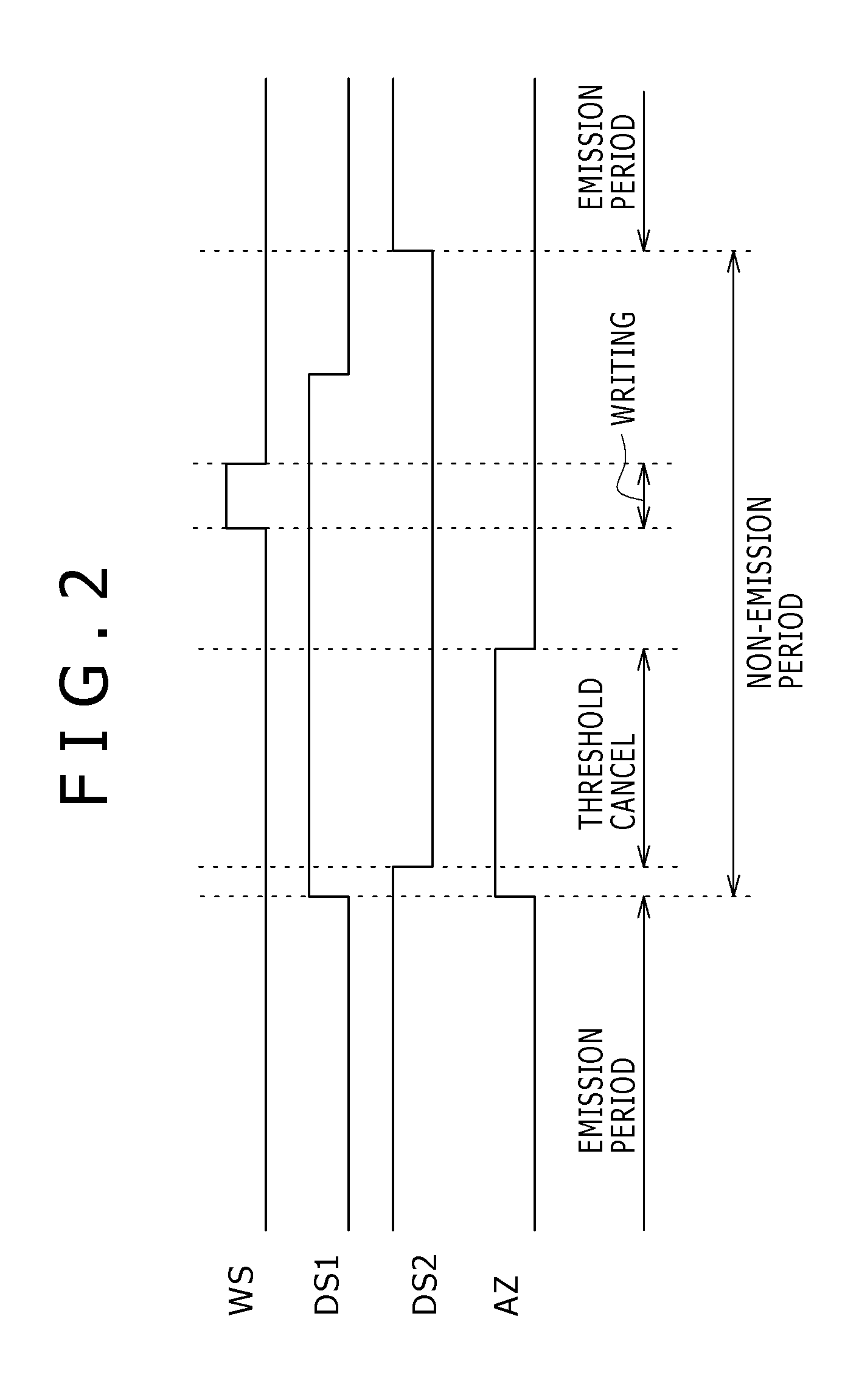
[0100]FIG. 12 is a timing chart showing the drive timing according to a first embodiment of the invention. The drive timing of the first embodiment is different from that of the above-described reference example in that in a non-emission period of the organic EL element 31 of the first embodiment, the active period during which the write signal WS output from the write scanning circuit 18 is at the “H” level is overlapped with the active period during which the drive signal DS output from the drive scanning circuit 19 is at the “H” level, and the overlapping period is defined as a mobility correction period. Other features are basically the same.

[0101] The operation before time t5 in the timing chart of FIG. 12 is the same as that in the reference example. Therefore, in the following, a description will be made on the operation at the time t5 and later, and particularly on the operation in the mobility correction period, i.e., the operation during the period from time t6 to time t7...

second embodiment

[0127] To address this problem, in an organic EL display according to a second embodiment of the invention, two-stage mobility correction is implemented in the following manner as shown in the timing chart of FIG. 18. Specifically, mobility correction with an intermediate grayscale is executed in the first half of a horizontal period during which the signal voltages Vsig_R, Vsig_G and Vsig_B are written (horizontal writing period), specifically, is executed at the beginning of the horizontal writing period. Subsequently, mobility correction with the signal voltages Vsig_R, Vsig_G and Vsig_B is executed in the latter half of the horizontal writing period, specifically, is executed at the end of the horizontal writing period.

[0128] Also in the organic EL display of the present embodiment, the write scanning circuit 18 and the drive scanning circuit 19 correspond to the driver set forth in the claims.

[0129] The operation in one horizontal period will be described below with reference...

application example of second embodiment

[0138] In the present embodiment, an intermediate grayscale level is supplied from the data line drive circuit 22 via the selector 24 to the data line 17. Alternatively, another configuration is also available in which, as shown in FIG. 19, precharge switches 25 are connected to e.g. the ends of the data lines 17 on the opposite side of the data line drive circuit 22 and an intermediate grayscale level is selectively supplied to the data lines 17 via the precharge switches 25. In this configuration, switching on / off of the precharge switches 25 is controlled by a precharge signal Tp that is active in the first half of the horizontal writing period as shown in FIG. 20.

[0139] The employment of the configuration to supply an intermediate grayscale level with use of the precharge switches 25 eliminates the need for the selector 24 to execute the operation for writing the intermediate grayscale level, and therefore offers advantages that a margin for the period for writing the signal vo...


PUM


Abstract

In a display in which pixel circuits each including a drive transistor, switching transistors and a capacitor are arranged in rows and columns, two-stage mobility correction is implemented in which mobility correction with an intermediate grayscale level (gray level) is executed before mobility correction is executed with an input signal (Vsig) level being written to the gate of the drive transistor when the switching transistor is in the conducting state. Thus, even if the mobility correction period is constant, mobility correction can be implemented for all the grayscales within the mobility correction period. This feature allows achievement of a uniform image quality free from streaks and unevenness attributed to variation in the mobility from pixel to pixel.

Description

CROSS REFERENCES TO RELATED APPLICATIONS [0001] This application contains subject matter related to Japanese Patent Application JP 2005-298497 filed with the Japanese Patent Office on Oct. 13, 2005, the entire contents of which being incorporated herein by reference. BACKGROUND OF THE INVENTION [0002] 1. Field of the Invention [0003] The present invention relates to a display and a method for driving a display, and particularly to a display in which pixel circuits each including an electro-optical element are arranged in rows and columns (in a matrix), and a method for driving the display. [0004] 2. Description of Related Art [0005] In recent years, development and commercialization of organic electro luminescence (EL) displays have been advanced. In the organic EL display, a large number of pixel circuits are arranged in a matrix, and each pixel circuit includes an organic EL element, which is a so-called current-driven light-emitting element of which emission luminance varies depe...

Claims


Application Information

Patent Timeline
Patent Type & Authority Applications(United States)
IPC IPC(8): G09G3/30H05B44/00
CPCG09G3/3233G09G2300/0819G09G2300/0842G09G2300/0861G09G2310/0248G09G2320/0233G09G2320/043
Inventor YAMAMOTO, TETSUROUCHINO, KATSUHIDEYAMASHITA, JUNICHI
Owner SONY CORP
Why Eureka
Try Eureka