Camera module using printed circuit board with step portion

Inactive Publication Date: 2007-05-24
SAMSUNG ELECTRO MECHANICS CO LTD
View PDF2 Cites 13 Cited by
  • Summary
  • Abstract
  • Description
  • Claims
  • Application Information

AI Technical Summary

Benefits of technology

[0016] An advantage of the present invention is that it provides a camera module using a PCB with a step portion, in which a step portion is formed along the edge of the PCB and the bottom portion of a housing is inserted and attached into the step portion. Accordingly, it is possible to prevent external light from penetrating through the adhesion portion between the housing and the PCB. Accordingly, it is possible to enhance the quality of image taken by the image sensor. In addition, the contact area between the housing and the PCB is increased, which makes it possible to enhance the assembly reliability of the camera module.
[0017] The present invention also provides a camera module comprising: a PCB on which an image sensor is mounted and along the edge of which a step portion is formed; a housing in which an IR filter is installed and a bottom peripheral portion of which is closely attached to the step portion of the PCB; and a lens barrel installed vertically in an upper portion of the housing and including a plurality of stacked lenses therein.
[0018] Additional aspect and advantages of the present general invent

Problems solved by technology

However, the epoxy may be insufficiently coated between the PCB and the housing.
In addition, the adhesive performance of the epoxy may degrade with the lapse of a l

Method used


Image

  • Camera module using printed circuit board with step portion
  • Camera module using printed circuit board with step portion
  • Camera module using printed circuit board with step portion

Examples


Embodiment Construction

[0035] Reference will now be made in detail to the embodiments of the present general inventive concept, examples of which are illustrated in the accompanying drawings, wherein like reference numerals refer to like elements throughout. The embodiments are described below in order to explain the present general inventive concept by referring to the figures.

[0036] Hereinafter, preferred embodiments of the present invention will be described in detail with reference to the accompanying drawings.

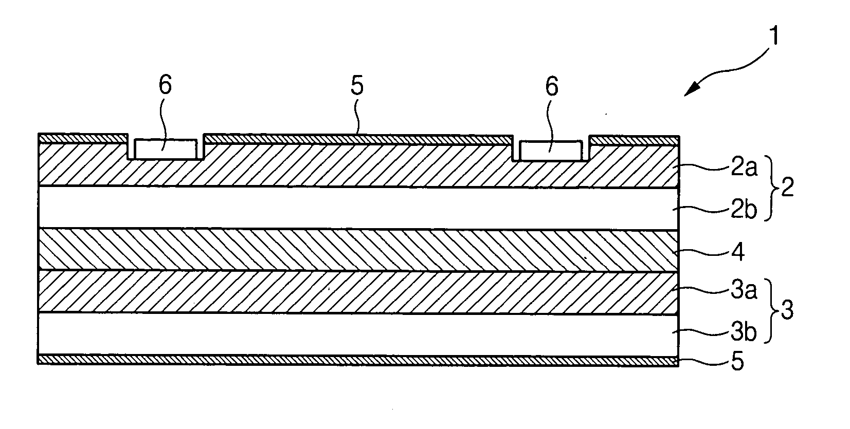
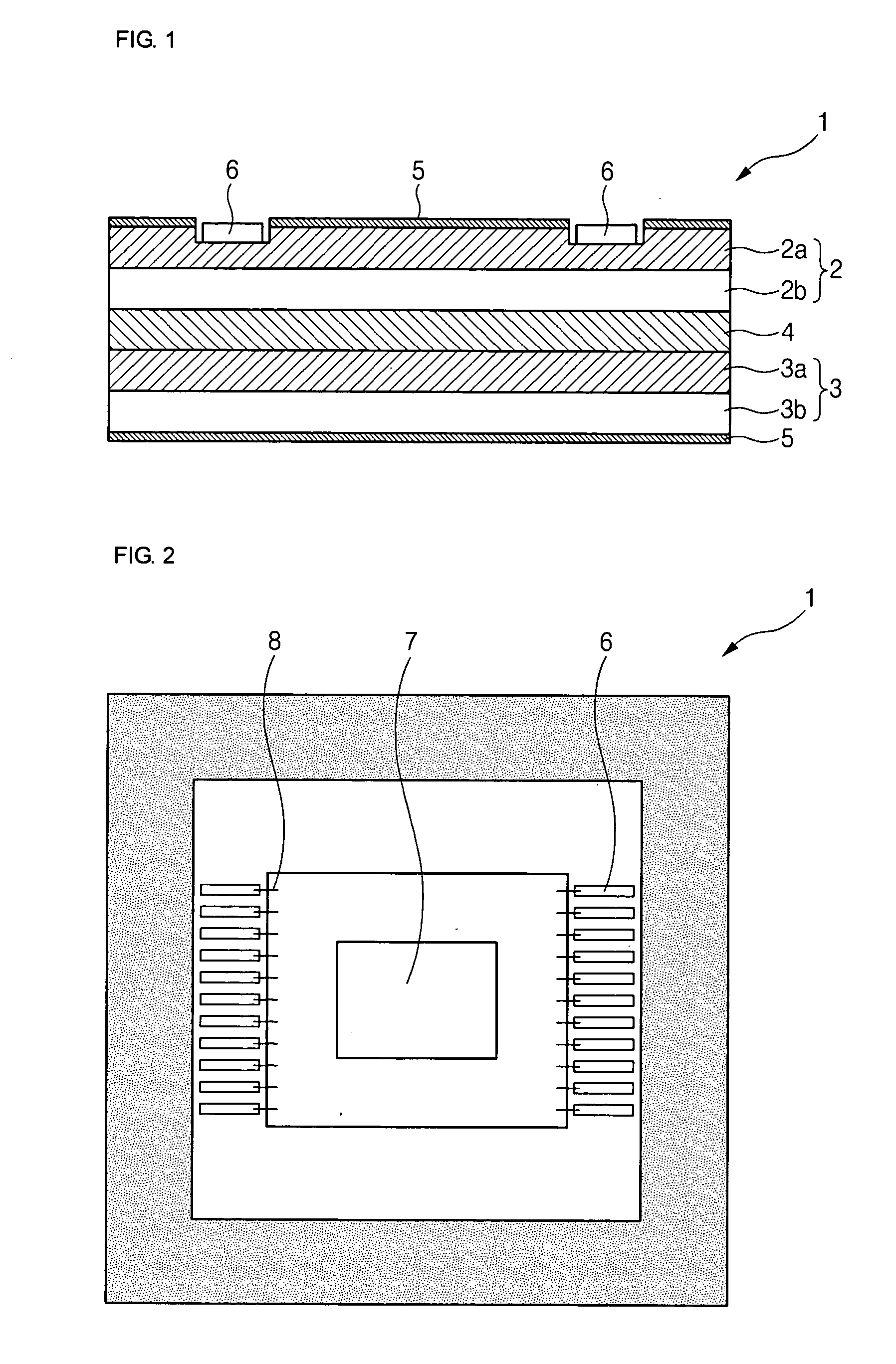
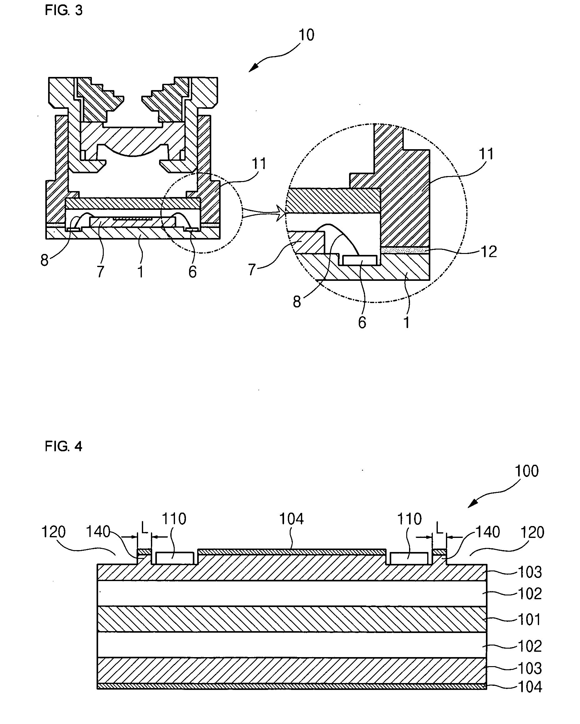
[0037]FIG. 4 is a sectional view of a PCB 100 according to an embodiment of the present invention, and FIG. 5 is a perspective view of the PCB 100 according to an embodiment of the present invention.

[0038] Referring to FIGS. 4 and 5, the PCB 100 includes a substrate main body 150 that has the shape of a rectangular plate. A plurality of pads 110 are formed on the substrate main body 150. An image sensor 130 is mounted on the central region of the substrate main body 150 in such a way that it ...


PUM


Abstract

Provided is a camera module using a PCB with a step portion. The camera module includes a PCB, a housing, and a lens barrel. The PCB includes a substrate main body, a plurality of pads, and a step portion. The substrate main body is formed of a stacked structure with the shape of a rectangular plate. The pads is formed on both sides of the top of the substrate main body and is electrically connected through wires to an image sensor mounted on a central portion of the top of the substrate main body. The step portion is formed at the peripheral edges of the pads. The housing has a bottom peripheral portion that is closely attached to the step portion of the PCB. The lens barrel is installed vertically in an upper region of the housing. Accordingly, it is possible to enhance the quality of image taken by the image sensor. In addition, the contact area between the housing and the PCB is increased to make it possible to enhance the assembly reliability of the camera module.

Description

CROSS-REFERENCE TO RELATED APPLICATIONS [0001] This application claims the benefit of Korean Patent Application No. 2005-112158 filed with the Korea Industrial Property Office on Nov. 23, 2005, the disclosure of which is incorporated herein by reference. BACKGROUND OF THE INVENTION [0002] 1. Field of the Invention [0003] The present invention relates to a camera module using a printed circuit board (PCB) with a step portion. In the camera module, a step portion is formed along the edge of the PCB and the bottom portion of a housing is inserted and attached into the step portion. Accordingly, it is possible to prevent external light from penetrating through the adhesion portion between the housing and the PCB. Accordingly, it is possible to enhance the quality of image taken by the image sensor. In addition, the contact area between the housing and the PCB is increased, which makes it possible to enhance the assembly reliability of the camera module. [0004] 2. Description of the Rela...

Claims


Application Information

Patent Timeline
IPC IPC(8): H05K1/00G03B17/02G03B30/00H01L23/12H04N5/225H04N5/335H05K1/02H05K3/28
CPCG03B17/00H01L27/14618H01L31/0203H01L31/0232H04N5/2253H04N5/2257H05K1/111H05K3/305H05K2201/09736H05K2201/09745H05K2203/049H01L2224/48091H01L2224/48227H01L2224/49175H01L2924/00014H01L2924/16195Y02P70/50H04N23/54H04N23/57H01L2924/00G02B7/00G02B7/02H04N23/00
Inventor KIM, GAB YONGLEE, SEUNG JU
Owner SAMSUNG ELECTRO MECHANICS CO LTD
Why Eureka
Try Eureka