Lithographic apparatus including a cleaning device and method for cleaning an optical element

a technology of cleaning device and optical element, applied in the field of lithographic apparatus, can solve the problems of sputtering effect being particularly problematic for radiation collectors, affecting the cleaning effect of other mirrors in the system, and affecting the cleaning effect of optical elements,

Inactive Publication Date: 2007-06-07
ASML NETHERLANDS BV
View PDF3 Cites 51 Cited by
  • Summary
  • Abstract
  • Description
  • Claims
  • Application Information

AI Technical Summary

Benefits of technology

[0009] It is another aspect of the invention to provide a method for cleaning an optical element of a lithographic apparatus. To that end, the invention relates to a method for cleaning of one or more optical elements of an EUV lithographic apparatus, the method including providing a cleaning device configured to provide a flow of hydrogen radicals, wherein the cleaning device includes a hydrogen radical source, and a flow tube in communication with the hydrogen radical sour

Problems solved by technology

These particles can be damaging to the collector and condenser mirrors which are generally multilayer mirrors or grazing incidence mirrors, with fragile surfaces.
The sputtering effect is particularly problematic for the radiation collector.
Other mirrors in the system are gen

Method used


Image

  • Lithographic apparatus including a cleaning device and method for cleaning an optical element
  • Lithographic apparatus including a cleaning device and method for cleaning an optical element
  • Lithographic apparatus including a cleaning device and method for cleaning an optical element

Examples


Embodiment Construction

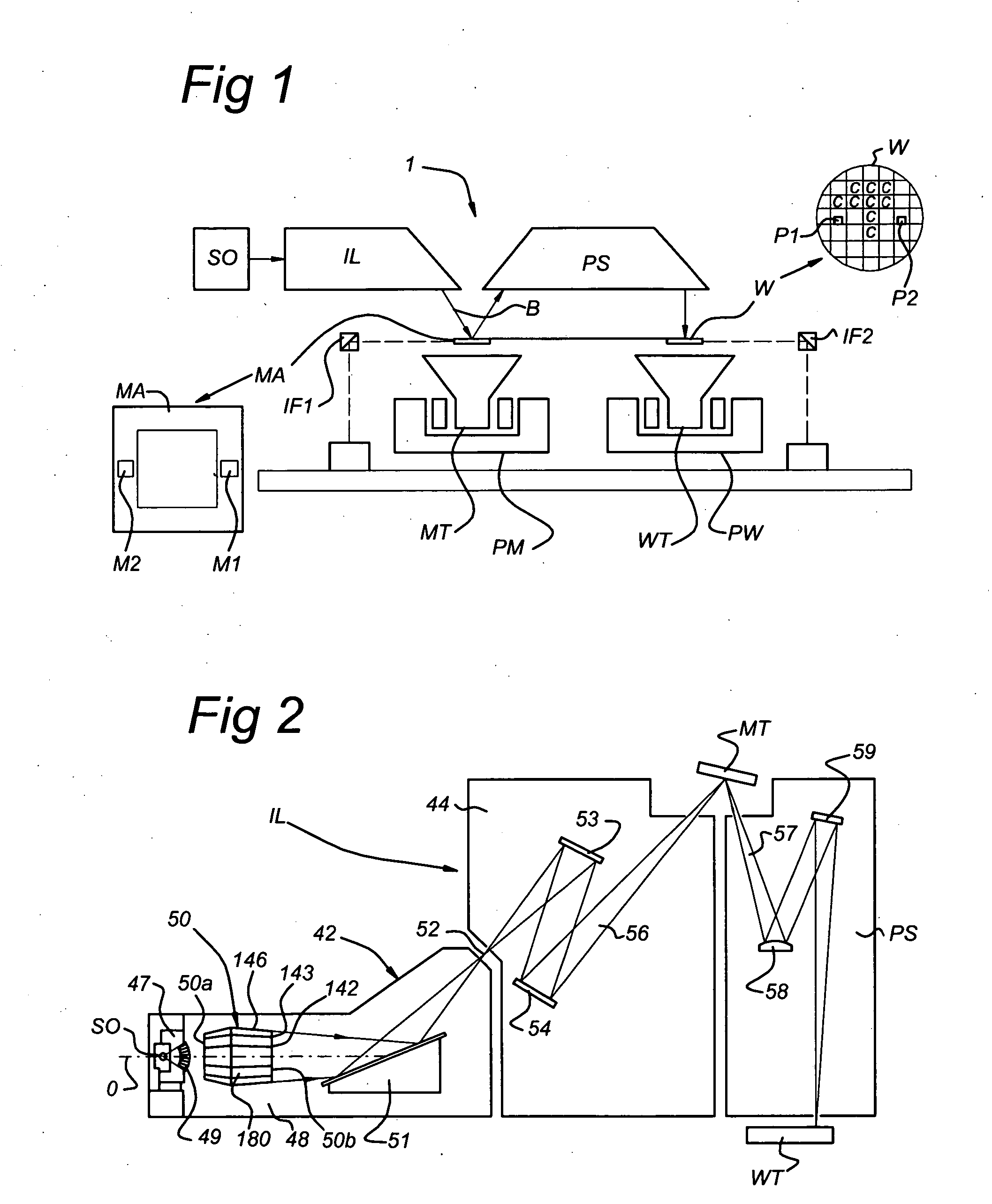
[0017]FIG. 1 schematically depicts a lithographic apparatus according to one embodiment of the invention. The apparatus includes an illumination system (illuminator) IL configured to condition a radiation beam B (e.g. UV radiation or EUV radiation). A support (e.g. a mask table) MT is configured to support a patterning device (e.g. a mask) MA and is connected to a first positioner PM configured to accurately position the patterning device in accordance with certain parameters. A substrate table (e.g. a wafer table) WT is configured to hold a substrate (e.g. a resist-coated wafer) W and is connected to a second positioner PW configured to accurately position the substrate in accordance with certain parameters. A projection system (e.g. a refractive projection lens system) PS is configured to project a pattern imparted to the radiation beam B by patterning device MA onto a target portion C (e.g. including part of, one, or more dies) of the substrate W.

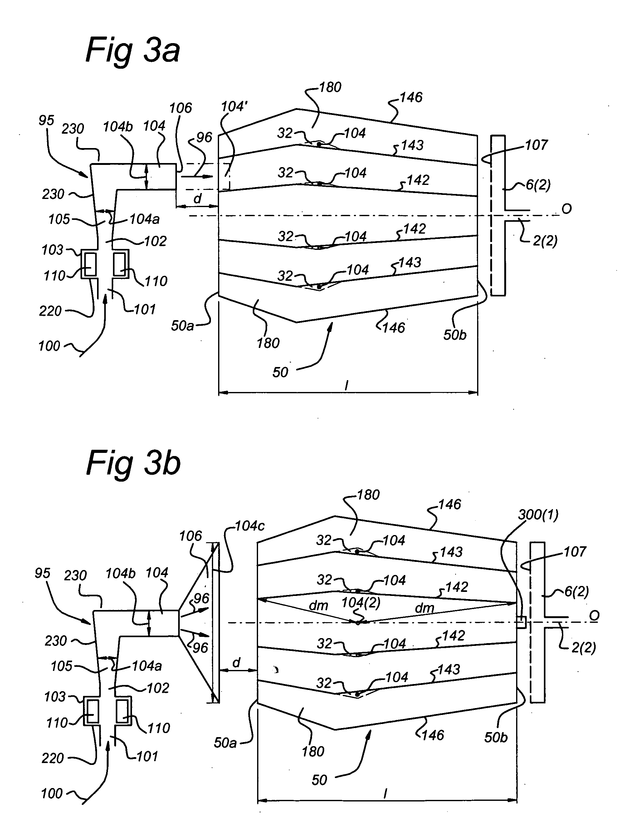
[0018] The illumination system m...


PUM

PropertyMeasurementUnit
Distanceaaaaaaaaaa
Distanceaaaaaaaaaa
Distanceaaaaaaaaaa

Abstract

An EUV lithographic apparatus includes an EUV radiation source, an optical element and a cleaning device. The cleaning device includes a hydrogen radical source and a flow tube in communication with the hydrogen radical source. The cleaning device is configured to provide a flow of hydrogen radicals and the flow tube is arranged to provide a hydrogen radical flow at a predetermined position within the lithographic apparatus, for example for cleaning a collector mirror.

Description

BACKGROUND OF THE INVENTION [0001] 1. Field of the Invention [0002] The present invention relates to a lithographic apparatus including a cleaning device and a method for cleaning optical elements. The present invention further relates to a cleaning device and to a method for manufacturing a cleaning device. [0003] 2. Background of the Invention [0004] A lithographic apparatus is a machine that applies a desired pattern onto a substrate, usually onto a target portion of the substrate. A lithographic apparatus can be used, for example, in the manufacture of integrated circuits (ICs). In that instance, a patterning device, which is alternatively referred to as a mask or a reticle, may be used to generate a circuit pattern to be formed on an individual layer of the IC. This pattern can be transferred onto a target portion (e.g. including part of, one, or several dies) on a substrate (e.g. a silicon wafer). Transfer of the pattern is typically via imaging onto a layer of radiation-sensi...

Claims


Application Information

Patent Timeline
IPC IPC(8): G03F7/20
CPCB82Y10/00G03F7/70033G03F7/70175G03F7/70883G03F7/70908G03F7/70916G03F7/70983G03F7/70933
Inventor VAN HERPEN, MAARTEN MARINUS JOHANNES WILHELMUSKLUNDER, DERK JAN WILFRED
Owner ASML NETHERLANDS BV
Why Eureka
Try Eureka