Error display system
- Summary
- Abstract
- Description
- Claims
- Application Information
AI Technical Summary
Benefits of technology
Problems solved by technology
Method used
Image
Examples
Embodiment Construction
[0035] Hereinafter, description will be given of one embodiment of the present invention with reference to the drawings.
[0036] In this embodiment, description will be given of, as an example, a case that a protective tape joining apparatus for joining a protective tape to a semiconductor wafer adopts an error display system.
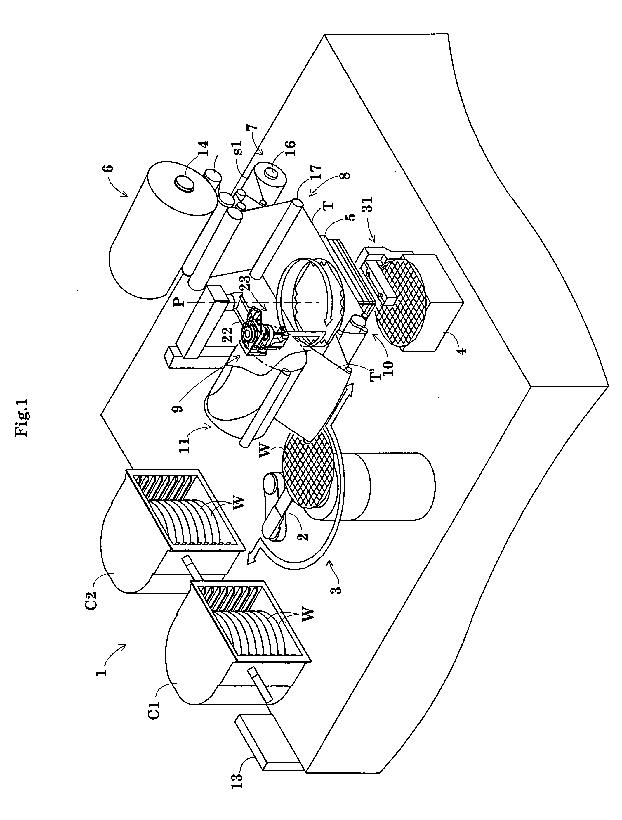
[0037]FIG. 1 is a perspective view illustrating a general configuration of the protective tape joining apparatus.
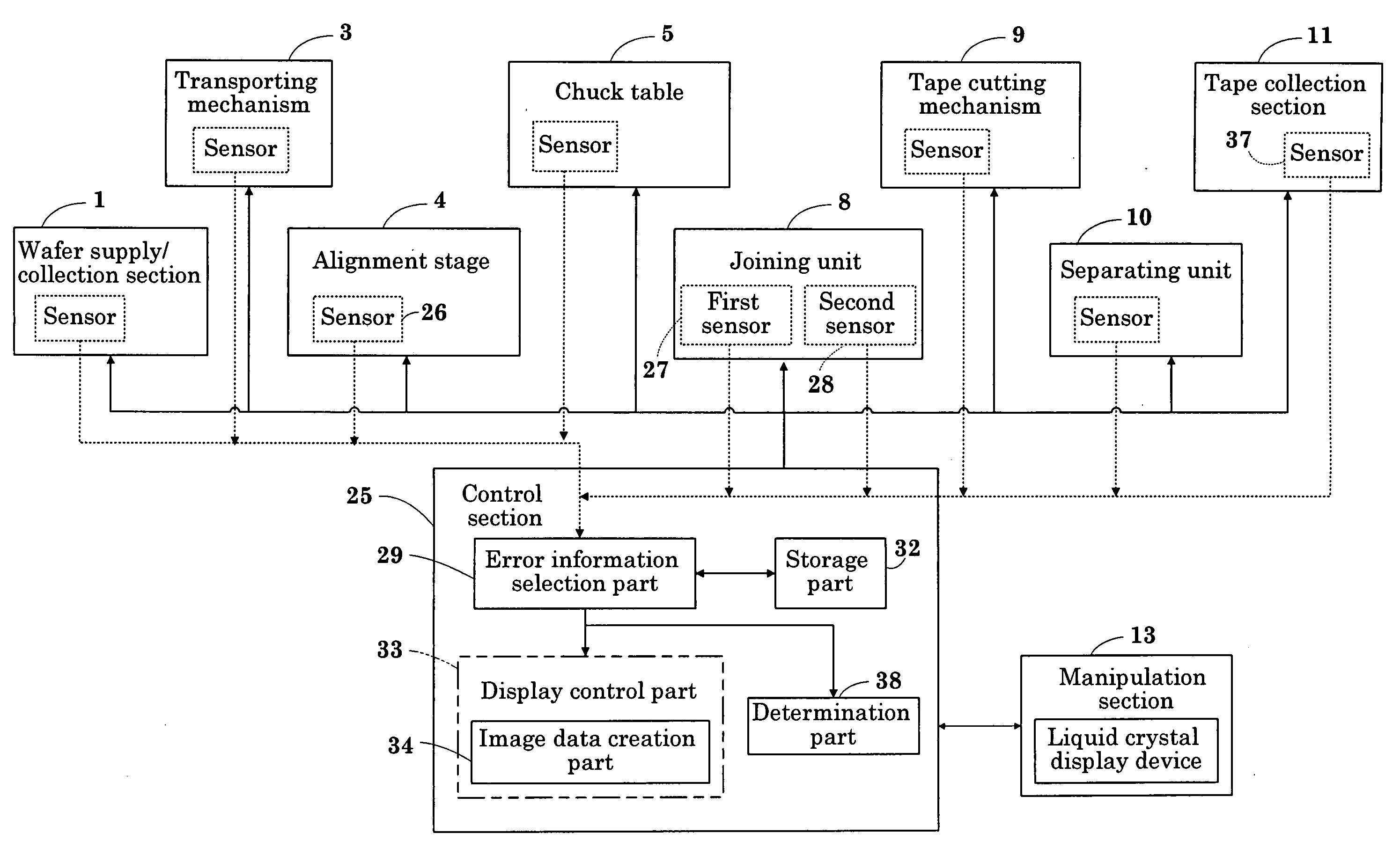
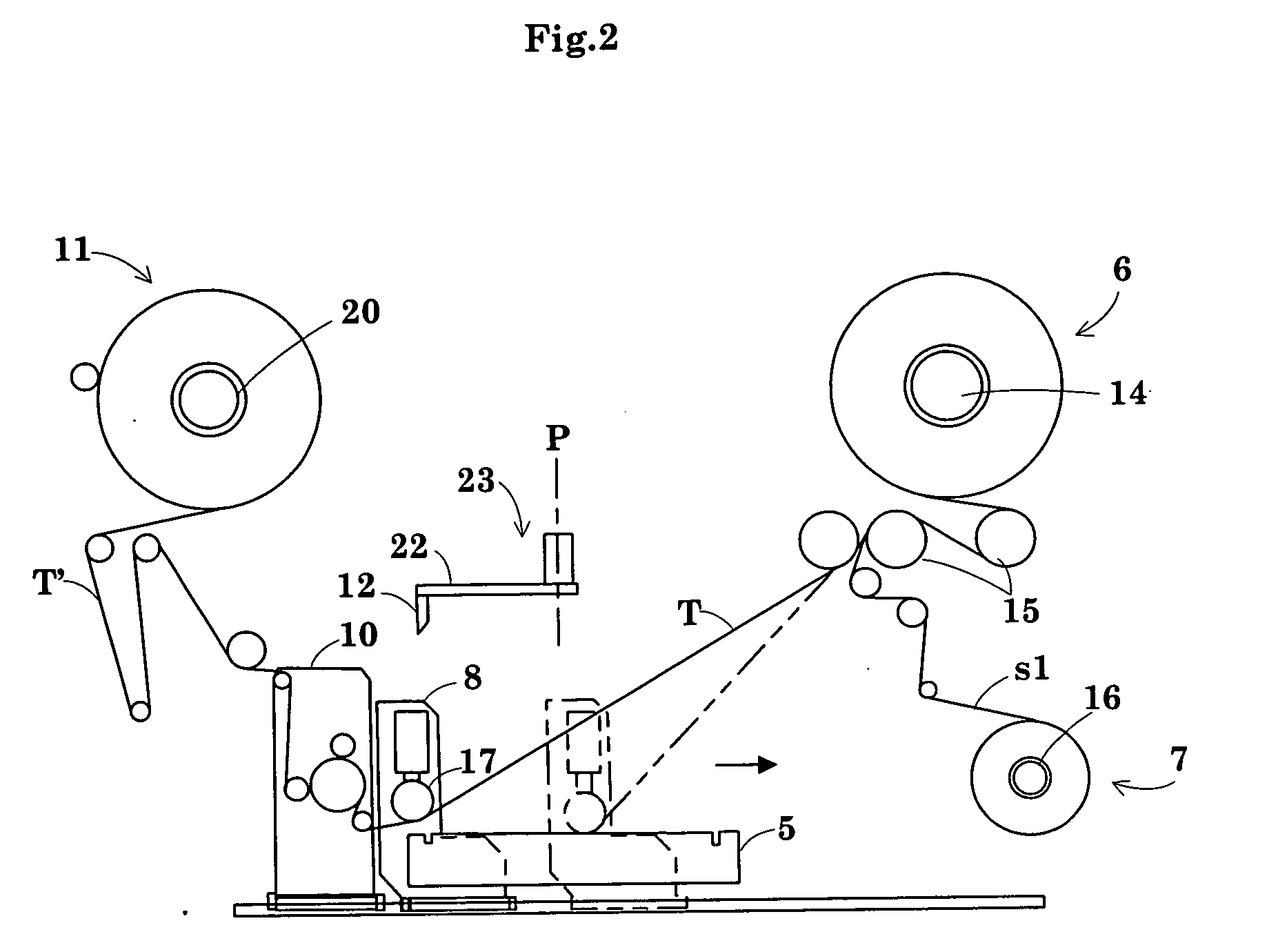
[0038] The protective tape joining apparatus comprises: a wafer supply / collection section 1 including a cassette C1 housing a semiconductor wafer (hereinafter, simply referred to as “wafer”) W which is a target of joining and a cassette C2 housing a wafer W′ having a protective tape T joined thereto; a wafer transporting mechanism 3 provided with a robot arm 2; an alignment stage 4; a chuck table 5 suction-holding a wafer W placed thereon; a tape supply section 6 supplying a protective tape T with a separator s1 toward the wafer W; a separator colle...
PUM
 Abstract
Description
Claims
Application Information


