
Organic semiconductor material, organic semiconductor structure and organic semiconductor apparatus

a technology of organic semiconductors and organic semiconductors, applied in the field of organic semiconductor materials, can solve the problems of solvent liquid crystallinity and solubility description, and achieve the effects of reducing lumo, reducing homo, and narrowing the band gap of organic semiconductor materials

Inactive Publication Date: 2007-06-07
DAI NIPPON PRINTING CO LTD
View PDF1 Cites 20 Cited by
  • Summary
  • Abstract
  • Description
  • Claims
  • Application Information

AI Technical Summary

Benefits of technology

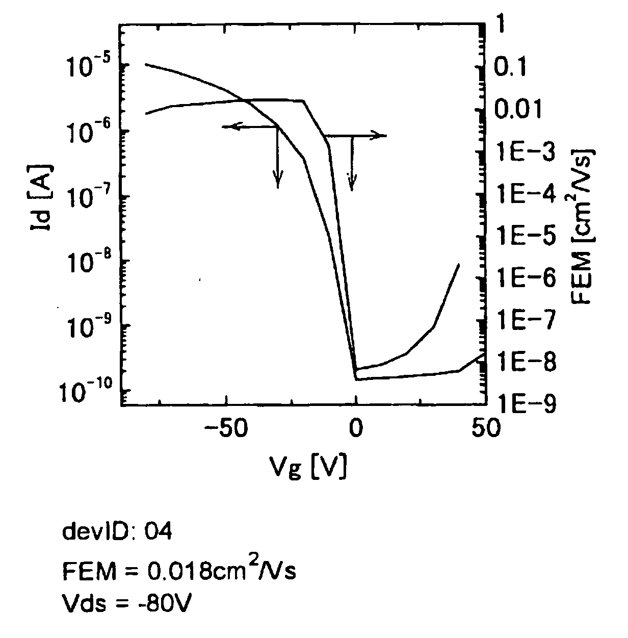
The present invention provides an organic semiconductor material that is stable under a film formation environment and can easily be brought to a film, for example, by coating. The material has high solubility in solvents and can form films with stable charge mobility in a wide service temperature range including room temperature. The invention also provides an organic semiconductor structure and an organic semiconductor device comprising the organic semiconductor material. The material has a chemical structure that delocalizes π electrons and suppresses the increase in ionization potential, making it less likely to undergo oxidation and the like. The invention solves the problem of developing an organic semiconductor material that is stable and easy to form films on.

Problems solved by technology

In these cases, however, film formation is carried out by vapor deposition, and, further, there is no description on liquid crystallinity and solubility in solvents of the thiazolothiazole derivatives.

Method used

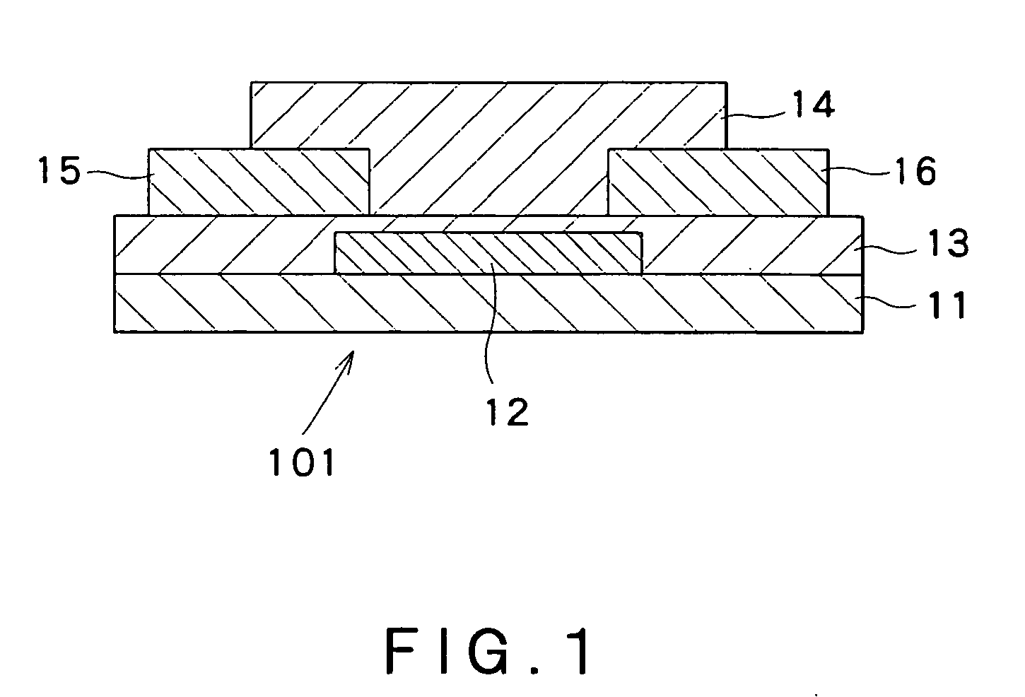

Image

  • Organic semiconductor material, organic semiconductor structure and organic semiconductor apparatus
  • Organic semiconductor material, organic semiconductor structure and organic semiconductor apparatus
  • Organic semiconductor material, organic semiconductor structure and organic semiconductor apparatus

Examples


example 1

[0062] In Example 1, an organic semiconductor material represented by chemical formula 1 wherein R1 and R2 represent a C8 identical straight chain alkyl group, was prepared.

Synthesis of 2-octylthiophene

[0063]

[0064] Thiophene (59.9 g, 0.713 mol) and dehydrated tetrahydrofran (hereinafter referred to as “THF”) (200 ml) were placed in a 1000-ml three-necked flask equipped with a 200-ml dropping funnel and a reflux tube. The solution was cooled to −78° C., and a solution (200 ml) of n-butyllithium (2.6 M) in n-hexane was added dropwise to the cooled solution over a period of about one hr. After the completion of the dropwise addition, the mixture was stirred at −78° C. for about one hr. Thereafter, the reaction temperature was raised to room temperature. At that temperature, the mixture was again stirred for one hr, and 1-bromooctane (91.8 g, 0.475 mol) was added dropwise thereto at 0° C. over a period of about one hr. After the completion of the dropwise addition, the reaction temper...

example 2

[0074] In Example 2, an organic semiconductor material, which is represented by chemical formula 2 wherein R3 and R4 represent a C10 identical straight chain alkyl group, was prepared.

Synthesis of 2-decylthiophene

[0075]

[0076] Thiophene (67.4 g, 0.801 mol) and THF (200 ml) were placed in a 1000-ml three-necked flask equipped with a 200-ml dropping funnel and a reflux tube. The solution was cooled to −78° C., and a solution (200 ml) of n-butyllithium (2.6 M) in n-hexane was added dropwise to the cooled solution over a period of about one hr. After the completion of the dropwise addition, the mixture was stirred at −78° C. for about one hr. Thereafter, the reaction temperature was raised to room temperature. At that temperature, the mixture was again stirred for one hr, and 1-bromodecane (118.0 g, 0.534 mol) was added dropwise thereto at 0° C. over a period of about one hr. After the completion of the dropwise addition, the reaction temperature was raised to room temperature, and, at...

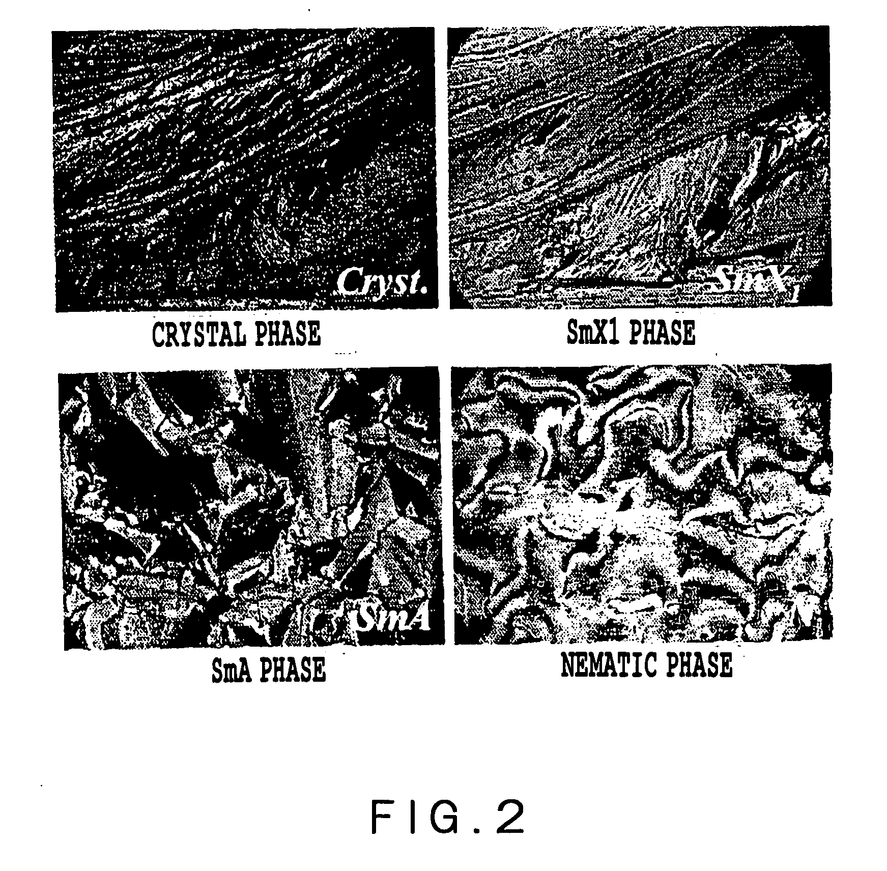

PUM


Abstract

The present invention is directed to the provision of a novel liquid crystalline organic semiconductor material that is highly stable under an film forming environment and, at the same time, can easily form a film, for example, by coating. The liquid crystalline organic semiconductor material is represented by chemical formula 1 wherein R1 and R2 represent an identical alkyl group having 7 to 20 carbon atoms: There is also provided a liquid crystalline organic semiconductor material characterized by being represented by chemical formula 2 wherein R3 and R4 represent an identical alkyl group having 7 to 20 carbon atoms:

Description

TECHNICAL FIELD [0001] The present invention relates to an organic semiconductor material comprising a liquid crystalline thiazolothiazole derivative, which organic semiconductor material is highly stable under an film forming environment and, at the same time, can easily form a film, for example, by coating, an organic semiconductor structure and an organic semiconductor device. BACKGROUND ART [0002] Attention has recently been drawn to studies on organic semiconductor structures using an organic semiconductor material, and application of organic semiconductor structures to various devices has been expected. Devices utilizable, for example, in large-area flexible display devices, for example, thin-film transistors (also known as “organic TFTs”), luminescent elements, and solar cells are being studied for such application. [0003] In order to utilize organic semiconductor structures on a practical level, the organic semiconductor layer formed of an organic semiconductor material shou...

Claims


Application Information

Patent Timeline
Patent Type & Authority Applications(United States)
IPC IPC(8): H01L29/08H01L51/40
CPCC09K19/3491C09K19/3497H01L51/0071H01L51/0076H01L51/0545H01L51/0558Y02E10/549H10K85/731H10K85/657H10K10/484H10K10/466
Inventor TOMINO, KENSUGAWARA, SHIGERUMAEDA, HIROKIMATSUOKA, MASANAO
Owner DAI NIPPON PRINTING CO LTD
Learn More