Imaging device

a technology of imaging device and pixel sensitivity, which is applied in the field of imaging device, can solve the problems of increasing the manufacturing cost of imaging device, unlikely to be able to normally operate, and flicker, and achieves the effects of reducing flicker, simple circuit structure, and simple structur

Inactive Publication Date: 2007-06-14
FUNAI ELECTRIC CO LTD
View PDF7 Cites 15 Cited by
  • Summary
  • Abstract
  • Description
  • Claims
  • Application Information

AI Technical Summary

Benefits of technology

[0012] It is an object of the present invention to provide an imaging device with reduced occurrence of flicker that can change the pixel sensitivity with an inexpensive and simple circuit structure without adding special circuit elements.
[0016] In the pixel downsampling read mode, the voltage of the first gate and the voltage of the second gate in each of the pixels to be discarded are brought to a high level, and subsequently the voltage of the first gate and the voltage of the second gate in each of the pixels to read a signal from are brought to a high level, so as to transfer charge, which is generated in the photoelectric conversion unit in each of the pixels to read a signal from, to the capacitance means and the photoelectric conversion unit in each of the pixels to be discarded. In the pixel downsampling read mode, not only the capacitance means but also channel portions of the transfer means and the photoelectric conversion units of the pixels to be discarded are used as capacitances for storing the signal charges transferred from the transfer means to lower potential of the capacitance means as compared with the case of using only the capacitance means as a capacitance for storing signal charges from the transfer means, thereby reducing sensitivity of the pixels.
[0017] Thus, in the imaging device according to the present invention, adjacent ones of the pixels use the capacitance means, the signal amplifying means, the reset means and the pixel selection means in common, so that the imaging device can be simplified in structure and reduced in manufacturing cost. Furthermore, in the pixel downsampling read mode, not only the capacitance means but also channel portions of the transfer means and the photoelectric conversion units in the pixels to be discarded are used as capacitances for storing signal charges transferred from the transfer means. Accordingly, it is possible to lower the potential of the capacitance means to reduce the sensitivity of the pixels, thereby reducing the occurrence of flicker as compared with the case of using only the capacitance means as a capacitance for storing signal charges transferred from the transfer means.
[0019] In this imaging device, only the voltage of the first gate is brought to a low level first when transferring the charge, which is generated in the photoelectric conversion unit in each pixel to read a signal from, to the capacitance means and the photoelectric conversion unit in each pixel to be discarded. Thus, the charge can be prevented from being transferred back to the photoelectric conversion unit in the each pixel to read a signal from.

Problems solved by technology

On the other hand, in high brightness mode where an image received by the imaging device is in a high brightness range, flicker is likely to occur.
In this high brightness mode, the imaging device is unlikely to be able to normally operate if the photodiode has a normal or long charge accumulation time (e.g. longer than a half period of a commercial AC power supply) with a normal or high pixel sensitivity.
This is a problem because it causes the circuit structure to be complicated, thereby increasing the manufacturing cost of the imaging device.

Method used


Image

  • Imaging device
  • Imaging device
  • Imaging device

Examples


Embodiment Construction

[0033] Embodiments of the present invention, as best mode for carrying out the invention, will be described hereinafter with reference to the drawings. The present invention relates to an imaging device with reduced occurrence of flicker. It is to be understood that the embodiments described herein are not intended as limiting, or encompassing the entire scope of, the present invention. Note that like parts are designated by like reference numerals, characters or symbols throughout the drawings.

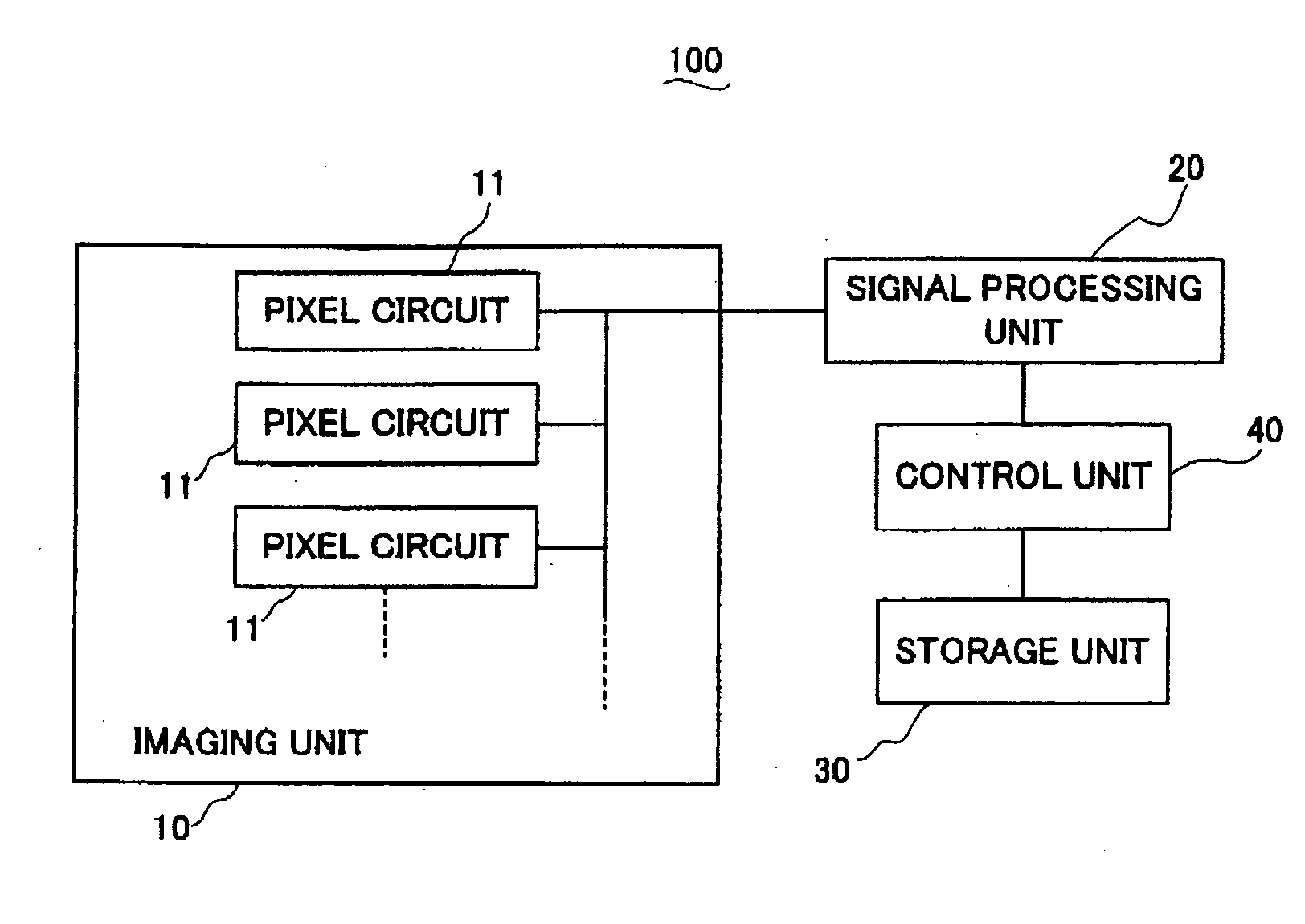
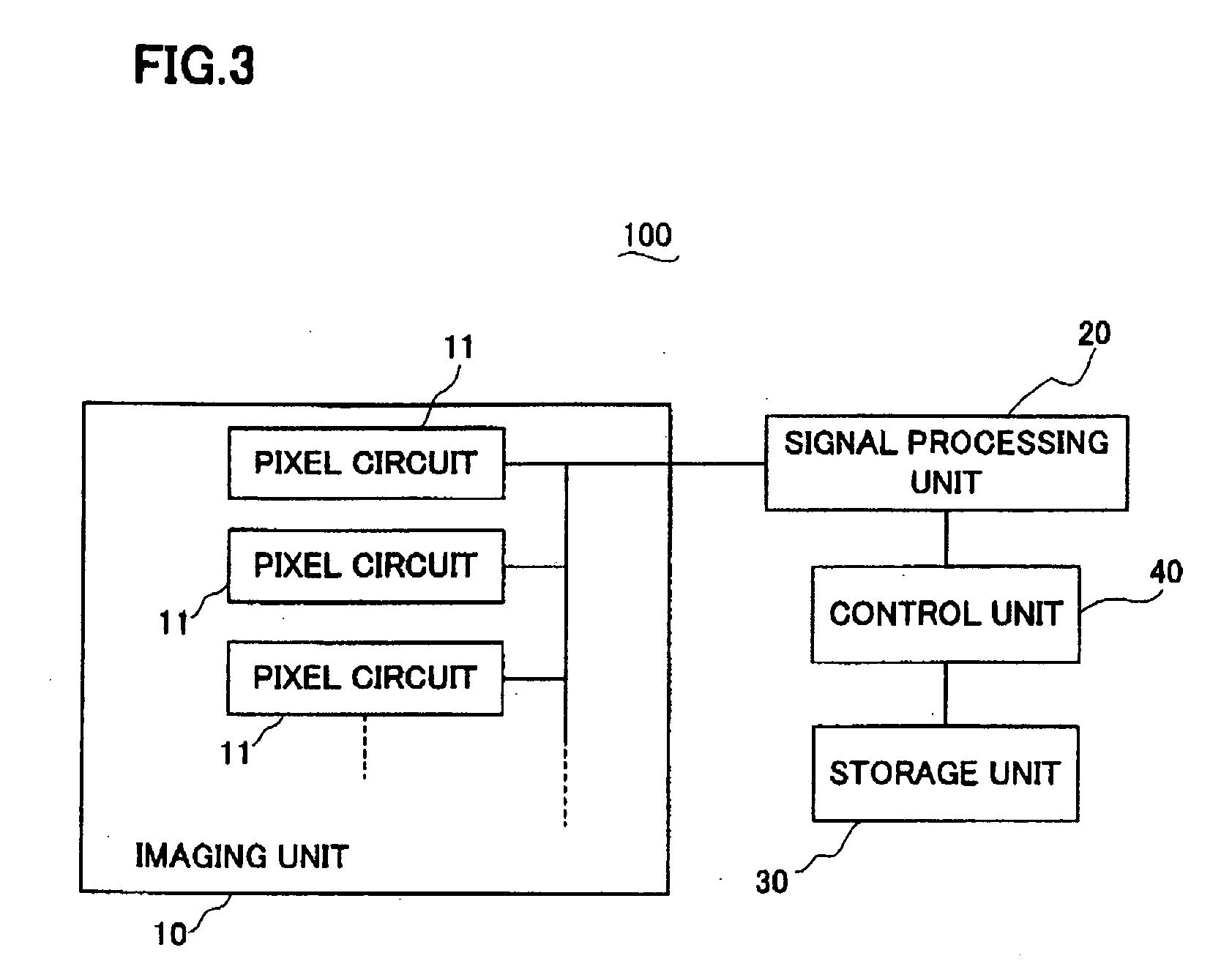
[0034] An embodiment of an imaging device according to the present invention will be described with reference to the annexed drawings. FIG. 3 is a schematic block diagram of an imaging device 100 according to the embodiment of the present invention. The imaging device 100 comprises: an imaging unit 10 having multiple pixels for imaging an image and outputting an electrical signal corresponding to the image; a signal processing unit 20 for processing the electrical signal output from the imag...


PUM


Abstract

Adjacent pixels in a pixel circuit of an imaging device use a primary capacitance, an amplifying transistor, a reset switch and a selection switch in common. Each pixel has a photodiode and a transfer switch having first and second gates provided on the photodiode side and the primary capacitance side, respectively. In a pixel downsampling read mode, the first and second gate voltages of each pixel to be discarded are brought to high level, and thereafter the first and second gate voltages of each pixel to be read are brought to high level, to transfer charge generated in the photodiode of the pixel to be read to the primary capacitance and the photodiode in each pixel to be discarded. This enables reduction of the potential of the primary capacitance, and hence reduction of the pixel sensitivity than using only the primary capacitance to store charge transferred from the transfer switch.

Description

BACKGROUND OF THE INVENTION [0001] 1. Field of the Invention [0002] The present invention relates to an imaging device with reduced occurrence of flicker. [0003] 2. Description of the Related Art [0004] Various studies have been made for an imaging device, particularly for a method of reading signals therein. For example, Japanese Laid-open Patent Publication 2000-165754 discloses a signal reading method for the purpose of increasing dynamic range. FIG. 1 and FIG. 2 correspond to FIG. 12 and FIG. 13 of the Patent Publication, respectively, which are a diagram of a pixel circuit of the fourth example described therein, and a timing chart showing the operation of the pixel circuit. The purpose of this signal reading method is not to reduce the occurrence of flicker, but to increase dynamic range as described above. However, since this method can be applied to reduce the occurrence of flicker under the illumination of a fluorescent lamp, this method will be described below as an exampl...

Claims


Application Information

Patent Timeline
Patent Type & Authority Applications(United States)
IPC IPC(8): H01L31/113H04N5/335H04N5/345H04N5/347H04N5/351H04N5/353H04N5/357H04N5/369H04N5/374
CPCH04N5/235H04N5/2357H04N5/335H04N5/3745H04N5/37457H04N23/745H04N23/70H04N25/00H04N25/778H04N25/77
Inventor OITA, MASAYATANAKA, HIROMICHIKIMATA, MASAFUMITERAKAWA, SUMIO
Owner FUNAI ELECTRIC CO LTD
Why Eureka
Try Eureka