Image processing circuit and image processing method

a technology which is applied in the field of image processing circuit and image processing method, can solve the problems of not detecting defects, defective color data is not corrected, and the light receiving elements of the other colors in the same pixel may include defects, so as to reduce color differences

Inactive Publication Date: 2007-06-21
SOCIONEXT INC
View PDF11 Cites 39 Cited by
  • Summary
  • Abstract
  • Description
  • Claims
  • Application Information

AI Technical Summary

Benefits of technology

[0009] The present invention provides an image processing circuit and an image processing method for correcting the value of a pixel included in color data to reduce color differences.

Problems solved by technology

Thus, if the light receiving element for a single color includes a defect, there is a high possibility of the light receiving elements for the other colors in the same pixel including a defect.
However, the above image processing circuit does not detect the defect when the data values for the other colors do not exceed the threshold value even if the defect for the single color is detected.
As a result, the defective color data is not corrected.
In such a case, the color data would differ from the actual color of the image subject and result in a color difference.

Method used


Image

  • Image processing circuit and image processing method
  • Image processing circuit and image processing method
  • Image processing circuit and image processing method

Examples


first embodiment

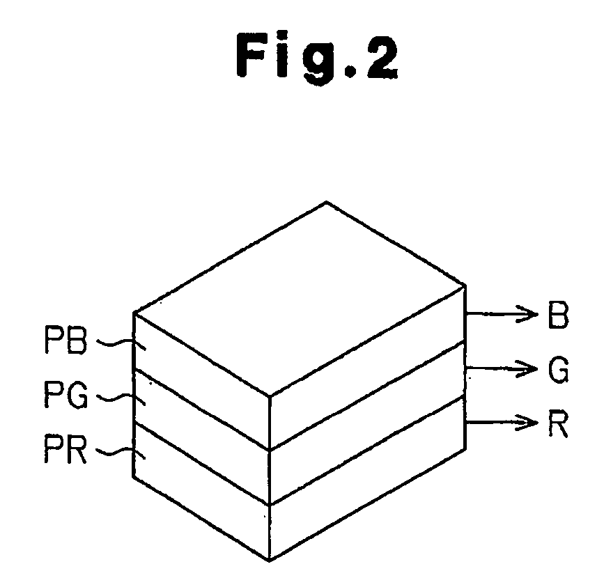
[0022] The image processing circuit 10 shown in FIG. 1 performs a defect determination process and a correction process based on the pixel value of a pixel (sub-pixel) that is subject to processing and a pixel value of at least one proximal pixel (sub-pixel) located proximal to the processing subject pixel. In the first embodiment, eight peripheral pixels (sub-pixels) adjacent to the processing subject pixel are used as the proximal pixels. For example, the red color data Rin includes the pixel value for a processing subject pixel R11 and the pixel values for eight peripheral pixels R00, R01, R02, R10, R12, R20, R21, and R22 (R00 to R22). That is, the color data Rin includes the pixel values for three rows and three columns of pixels. Based on the pixel value for the pixel R11 and the pixel values for the pixels R00 to R22, the image processing circuit 10 determines whether or not the processing subject pixel R11 includes a defect. When the pixel R11 includes a defect, the image pro...

second embodiment

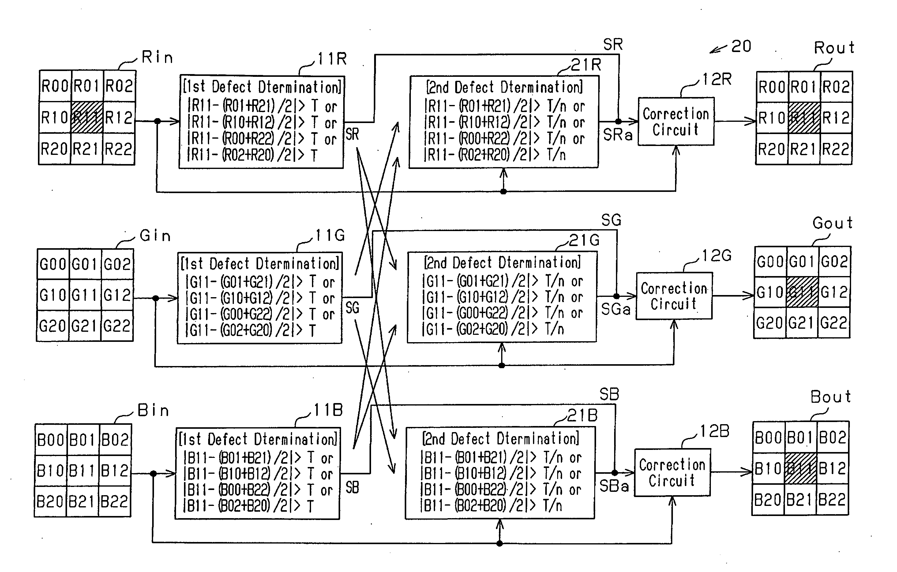
[0035] An image processing circuit 20 according to the present invention will now be discussed with reference to FIG. 3.

[0036] Referring to FIG. 3, the image processing circuit 20 includes first defect determination circuits 11R, 11G, and 11B, second defect determination circuits 21R, 21G, and 21B, and correction circuits 12R, 12G, and 12B corresponding to red, green, and blue, respectively. First and second threshold values are set beforehand for the first and second defect determination circuits, respectively.

[0037] In the same manner as the first embodiment, the first defect determination circuits 11R, 11G, and 11B perform a first determination process to determine whether or not the processing subject pixels R11, G11, and B11 include a defect based on the corresponding color data Rin, Gin, and Bin. Then, the first defect determination circuits 11R, 11G, and 11B generate first determination signals SR, SG, and SB, respectively.

[0038] When the processing subject pixel for a diff...


PUM

PropertyMeasurementUnit
coloraaaaaaaaaa
thresholdaaaaaaaaaa
color dataaaaaaaaaaa

Abstract

A circuit and method for processing an image to correct the pixel value of a sub-pixel included in color data to reduce color differences. The image processing circuit includes a plurality of defect determination circuits respectively corresponding to a plurality of sub-pixels (colors). Each defect determination circuit determines whether or not the corresponding sub-pixel, or first sub-pixel, includes a defect and generates a determination signal. The defect determination circuits provide each of a plurality of correction circuits respectively corresponding to a plurality of sub-pixels (colors) with the determination signals. Each correction circuit generates a corrected value for the corresponding first sub-pixel when at least one of the determination signal is indicative of a defect.

Description

CROSS-REFERENCE TO RELATED APPLICATIONS [0001] This application is based upon and claims the benefit of priority from the prior Japanese Patent Application No. 2005-366970, filed on Dec. 20, 2005, the entire contents of which are incorporated herein by reference. BACKGROUND OF THE INVENTION [0002] The present invention relates to an image processing circuit and an image processing method, and more particularly, to a circuit and method for correcting pixel defects included in color image data. [0003] Solid state imaging devices, such as a CCD, are nowadays often used. A solid state device includes a matrix of pixels that receive light. Each pixel (i.e., sub-pixel) receives red (R), green (G), and blue (B) light and generates image data. The image data of the pixels configures color image data. The pixels of a solid-state imaging device may include structural defects due to factors resulting from the manufacturing process. Thus, the image data generated by a pixel having a defect must...

Claims


Application Information

Patent Timeline
Patent Type & Authority Applications(United States)
IPC IPC(8): G03F3/08H04N5/335H04N5/367H04N5/372H04N5/374H04N5/376H04N9/07
CPCH04N1/401H04N5/3675G06T5/005G06T5/20G06T2207/10024H04N25/683H04N23/12H04N23/13
Inventor IGURA, KOUICHIFUKUOKA, TOMOHIRO
Owner SOCIONEXT INC
Why Eureka
Try Eureka