Micro-fabricated device with thermoelectric device and method of making

a thermoelectric device and micro-fabricated technology, applied in semiconductor devices, semiconductor/solid-state device details, electronic beam carrier recording, etc., can solve the problems of significant increase in chip heat flux, significant rise in power dissipation, and destruction or damage of silicon-based devices on which microprocessors are based

Inactive Publication Date: 2007-07-05
MCKINNELL JAMES C +2
View PDF17 Cites 23 Cited by
  • Summary
  • Abstract
  • Description
  • Claims
  • Application Information

AI Technical Summary

Problems solved by technology

To a large extent these advances have been made possible by increases in packaging density which has led to a significant rise in power dissipation that in turn leads to a substantial increase in chip heat flux.
Today's high performance computing devices, if left unaltered will result in peak temperatures that will destroy or damage the silicon-based devices on which microprocessors are typically formed.
However, in other cases good thermal conduction is limited by the opposing need for electrical isolation.
The end result is an electronic device whose performance is compromised.
The inability to control thermal losses can both, result in a significant increase in power consumption as well as less than optimum performance.
In addition, sub-ambient cooling of electronic devices, such as, for example, high-end mainframe computer systems, typically, utilize refrigeration based systems which significantly add to the complexity and cost.

Method used


Image

  • Micro-fabricated device with thermoelectric device and method of making
  • Micro-fabricated device with thermoelectric device and method of making
  • Micro-fabricated device with thermoelectric device and method of making

Examples


Embodiment Construction

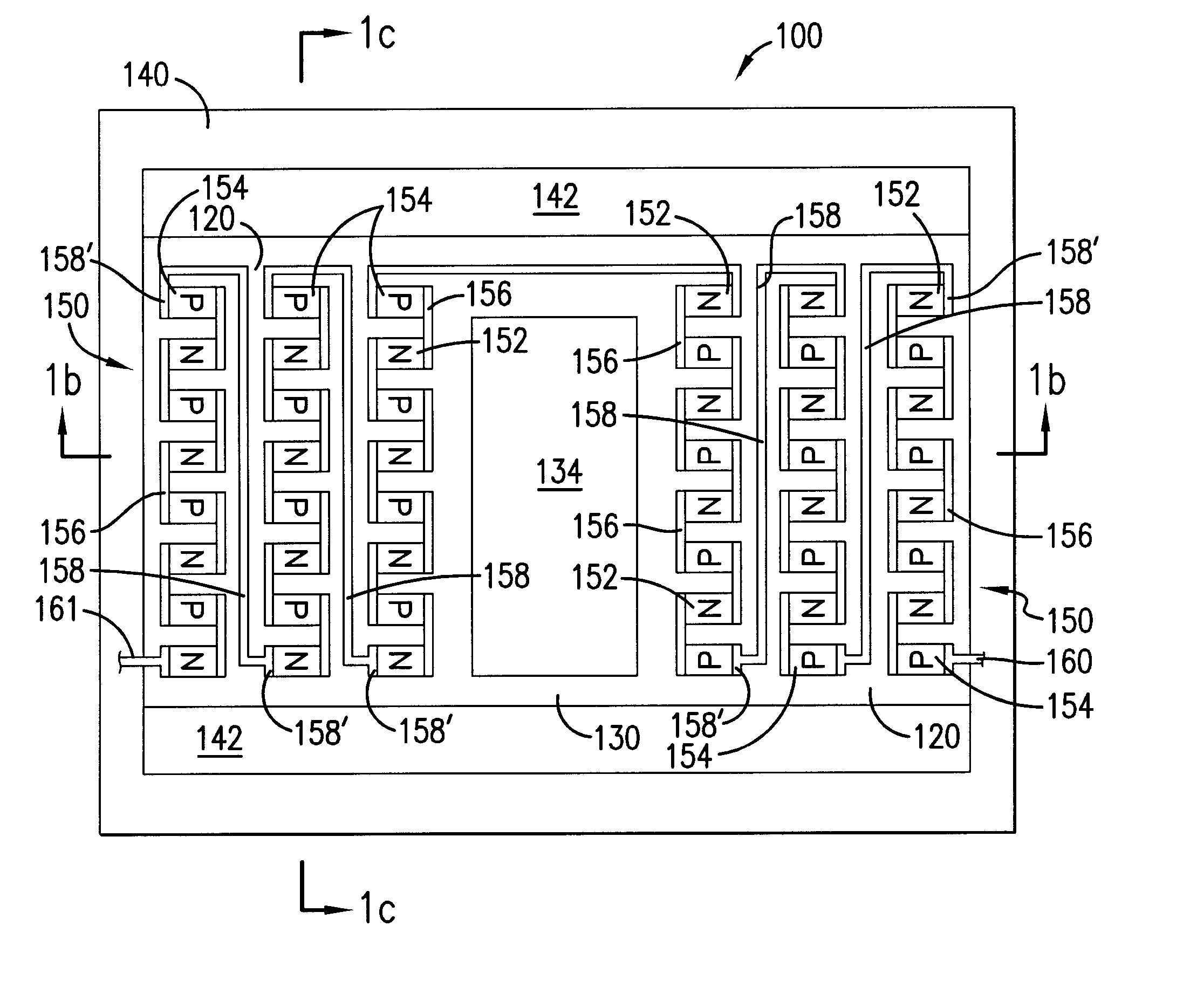
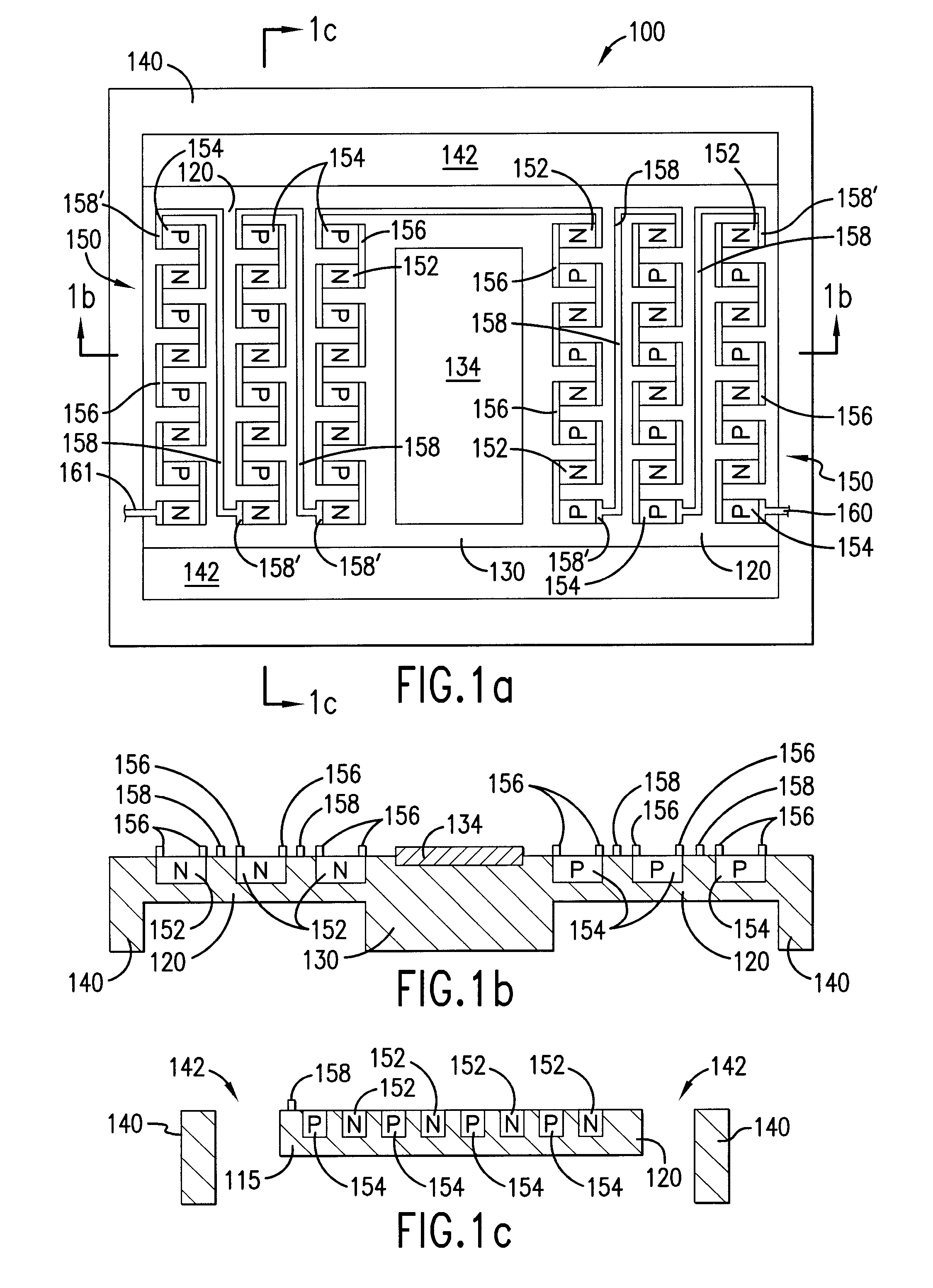
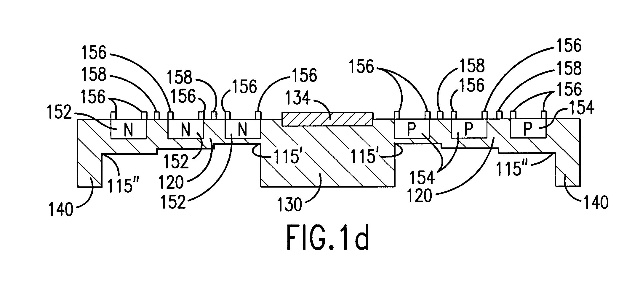
[0021] Referring to FIG. 1a, a top view is shown of an embodiment of micro-fabricated device 100 of the present invention. In this embodiment, thermally isolating structure 120 includes thermoelectric device 150 that provides selective heating or cooling of device substrate 130. In addition, thermally isolating structure 120 reduces the thermal conductivity between device substrate 130 and support structure 140 while also providing mechanical support. Device substrate 130 is disposed, within aperture 142 formed in support structure 140.

[0022] In this embodiment, active device 134 is disposed on device substrate 130. Active device 134 includes, for example, various transistors (including thin-film-transistor (TFT) technology using polysilicon on glass substrates), diodes, logic cells, as well as sensors, transducers, electron emitters, bolometers, and superconductoring high Q RF filters to name just a few of the many active devices that may be utilized in the present invention eithe...


PUM

PropertyMeasurementUnit
temperatureaaaaaaaaaa
thicknessaaaaaaaaaa

Abstract

A micro-fabricated device, includes a support structure having an aperture formed therein, and a device substrate disposed within the aperture. The micro-fabricated device further includes a thermally isolating structure thermally coupling the device substrate to the support structure. The thermally isolating structure includes at least one n-doped region and at least one p-doped region formed on or in the thermally isolating structure and separated from each other. In addition, the thermally isolating structure includes an electrical interconnect connecting at least one n-doped region and at least one p-doped region, forming an integrated thermoelectric device.

Description

CROSS-REFERENCE TO RELATED APPLICATIONS [0001] This application is a continuation application and claims the benefit and priority of U. S. patent application Ser. No. 10 / 353632 filed Jan. 29, 2003.BACKGROUND Description of the Art [0002] Over the past decade, the demand for cheaper and higher performance electronic devices has led to a growing need to manufacture electronic devices having lower power consumption as well as improved thermal efficiency. Microprocessors are a good example of the ever-increasing demands on power consumption and thus the need to better handle power dissipation. To a large extent these advances have been made possible by increases in packaging density which has led to a significant rise in power dissipation that in turn leads to a substantial increase in chip heat flux. Today's high performance computing devices, if left unaltered will result in peak temperatures that will destroy or damage the silicon-based devices on which microprocessors are typically ...

Claims


Application Information

Patent Timeline
Patent Type & Authority Applications(United States)
IPC IPC(8): H01L23/34G11B9/10H01L35/32H01L23/38H01L35/14H01L35/34
CPCG11B9/10H01L23/38H01L35/32H01L2924/09701H01L2924/10158H01L2924/0002Y10S257/93H01L2924/00H10N10/17
Inventor MCKINNELL, JAMES C.LIEBESKIND, JOHNCHEN, CHIEN-HUA
Owner MCKINNELL JAMES C
Why Eureka
Try Eureka