Connection verification technique

a verification technique and connection technology, applied in the field of electronic devices, can solve the problems of increasing the difficulty of identi.l.ving soldering, jtag requires extra devices, incomplete and expensive implementation, etc., and achieves the effect of convenient testing and efficient verification of connectivity

Active Publication Date: 2007-07-05
MICRON TECH INC
View PDF24 Cites 14 Cited by
  • Summary
  • Abstract
  • Description
  • Claims
  • Application Information

AI Technical Summary

Benefits of technology

[0011] Embodiments of the present invention are generally related to testing the interconnections between an I / C device and a mounting surface. In some embodiments, a connection pad of a memory device is electrically coupled via a test path to at least one other connection pad of the device to establish a temporary current path to facilitate testing. In other embodiments, a connection pad of a printed circuit board is similarly coupled to at least one other connection pad of the circuit board. As discussed below, a continuity test may then be performed to verify proper connections at these connection pads. Once continuity testing is complete, the test path between connection pads may be disabled to avoid interfering with operation of the memory device. In some embodiments, the presently disclosed techniques allow for efficient verification of the connectivity of all device interconnections to a printed circuit board when mounted to a surface of the circuit board.

Problems solved by technology

Once the BGA package is secured to a PCB or other device, however, the package itself obscures the connections between the package and the PCB or device, which increases the difficulty associated with identi.l.ving soldering faults, such as electrical shorts and opens, and generally verifying that the package is properly connected.
While various x-ray machines and special microscopes have been developed in an attempt to overcome some of these difficulties, it will be appreciated that these solutions are incomplete and expensive to implement.
However, JTAG requires extra device interconnections, adds die size, is time consuming, and may impact loading to higher speed I / O.
Further, JTAG does not support testing of certain connections, such as power and ground connections.

Method used


Image

  • Connection verification technique
  • Connection verification technique
  • Connection verification technique

Examples


Embodiment Construction

[0023] One or more specific embodiments of the present invention will be described below. In an effort to provide a concise description of these embodiments, not all features of an actual implementation are described in the specification. It should be appreciated that in the development of any such actual implementation, as in any engineering or design project, numerous implementation-specific decisions must be made to achieve the developers' specific goals, such as compliance with system-related and business-related constraints, which may vary from one implementation to another. Moreover, it should be appreciated that such a development effort might be complex and time consuming, but would nevertheless be a routine undertaking of design, fabrication, and manufacture for those of ordinary skill having the benefit of this disclosure.

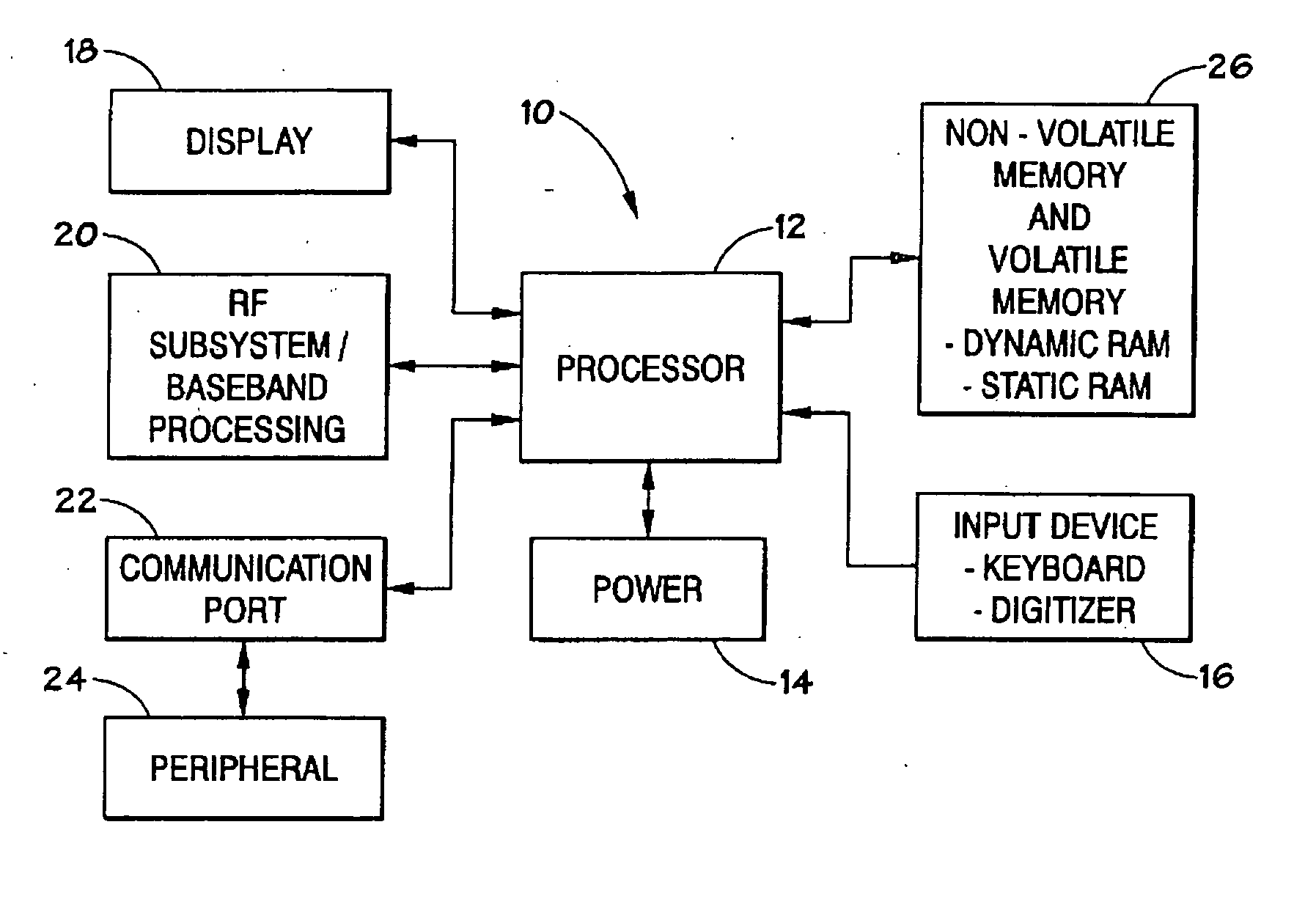
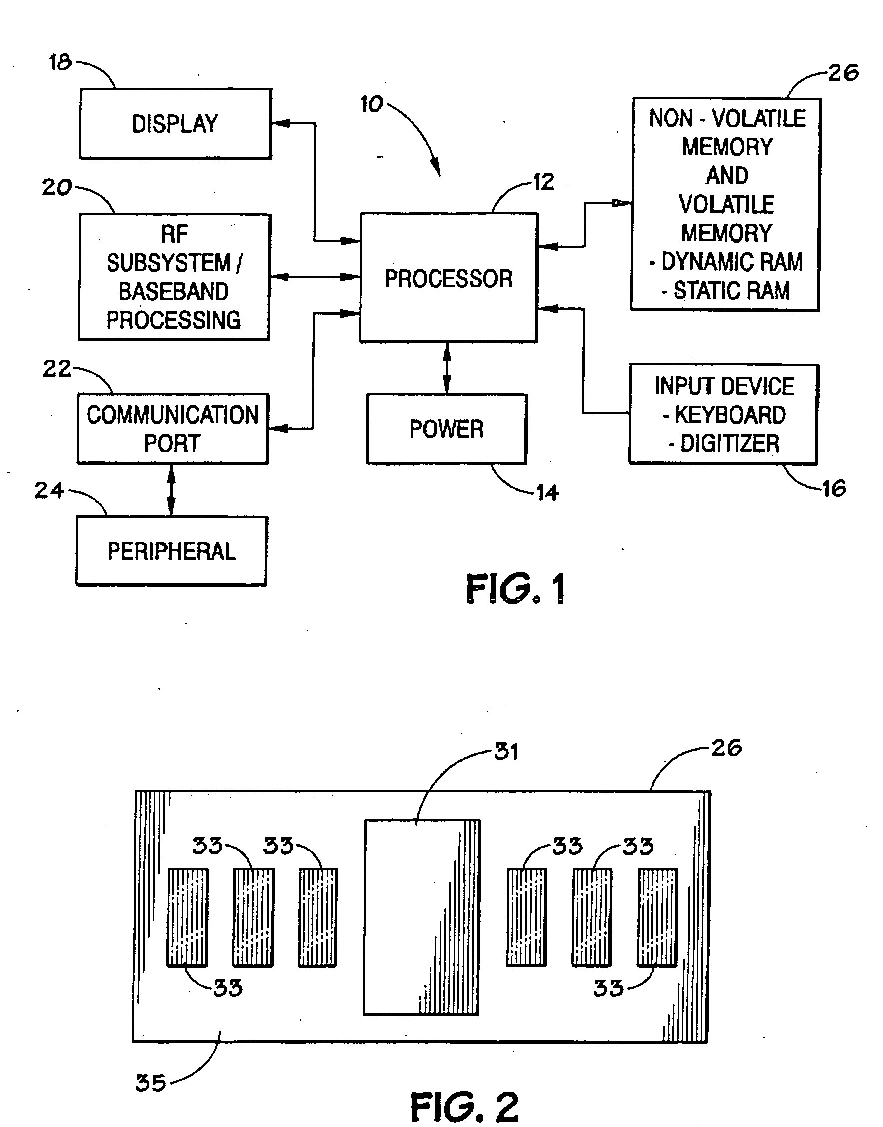
[0024] Turning now to the drawings, FIG. 1 is a block diagram of an electronic system containing integrated circuit devices that may employ embodiments ...


PUM

PropertyMeasurementUnit
resistanceaaaaaaaaaa
conductiveaaaaaaaaaa
electricalaaaaaaaaaa

Abstract

Embodiments of the present invention are generally directed to testing connections of a memory device to a circuit board or other device. In one embodiment, a memory device that is configured to facilitate continuity testing between the device and a printed circuit board or other device is disclosed. The memory device includes a substrate and two connection pads that are electrically coupled to one another via a test path. A system and method for testing the connections between a memory device and a circuit board or other device are also disclosed.

Description

BACKGROUND OF THE INVENTION [0001] 1. Field of the Invention [0002] The present invention relates generally to electronic devices, such as memory devices. More particularly, the present invention relates to a device and method for efficiently testing interconnections of electronic devices. [0003] 2. Description of the Related Art [0004] This section is intended to introduce the reader to various aspects of art that may be related to various aspects of the present invention, which are described and / or claimed below. This discussion is believed to be helpful in providing the reader with background information to facilitate a better understanding of the various aspects of the present invention. Accordingly, it should be understood that these statements are to be read in this light, and not as admissions of prior art. [0005] Microprocessor-controlled circuits are used in a wide variety of applications. Such applications include personal computers, control systems, telephone networks, an...

Claims


Application Information

Patent Timeline
Patent Type & Authority Applications(United States)
IPC IPC(8): G01R31/02
CPCG01R31/048H05K1/0268H05K1/111H05K3/3436H05K2201/09663H05K2201/09809Y10T29/49128H05K2203/163H05K2203/175B23K1/0016Y10T29/49004Y10T29/4913Y10T29/49144H05K2201/10734G01R31/71H01L2224/0401H01L2224/16227H01L2224/05551H01L2224/05552Y02P70/50H01L2924/00012G01R31/307G01R31/28
Inventor KINSLEY, THOMAS
Owner MICRON TECH INC
Why Eureka
Try Eureka