Conductive carbon nanotube tip, probe having the conductive carbon nanotube tip, and method of manufacturing the conductive carbon nanotube tip

a technology of conductive carbon nanotubes and carbon nanotubes, which is applied in the direction of material analysis using wave/particle radiation, instruments, nuclear engineering, etc., can solve the problems of inability to properly use a conductive tip for efm, mfm and scm, and the diameter of the tip is difficult to less than 100 nm, so as to improve the resolution and endurance of the device, and the effect of the same conductivity

Active Publication Date: 2007-07-19
SAMSUNG ELECTRONICS CO LTD
View PDF3 Cites 32 Cited by
  • Summary
  • Abstract
  • Description
  • Claims
  • Application Information

AI Technical Summary

Benefits of technology

[0009]The present invention may provide a conductive carbon nanotube tip that has a nano-scale diameter and the same conductiv

Problems solved by technology

However, due to the limitations in the material and the manufacturing process, it commonly is difficult to reduce the diameter of the tip to less than 100 nm.
Therefore, it is difficult to analyze a grain size

Method used


Image

  • Conductive carbon nanotube tip, probe having the conductive carbon nanotube tip, and method of manufacturing the conductive carbon nanotube tip
  • Conductive carbon nanotube tip, probe having the conductive carbon nanotube tip, and method of manufacturing the conductive carbon nanotube tip
  • Conductive carbon nanotube tip, probe having the conductive carbon nanotube tip, and method of manufacturing the conductive carbon nanotube tip

Examples


Embodiment Construction

[0025]The present invention will now be described more fully with reference to the accompanying drawings, in which exemplary embodiments of the invention are shown. In the drawings, the thicknesses and diameters of elements are exaggerated for clarity.

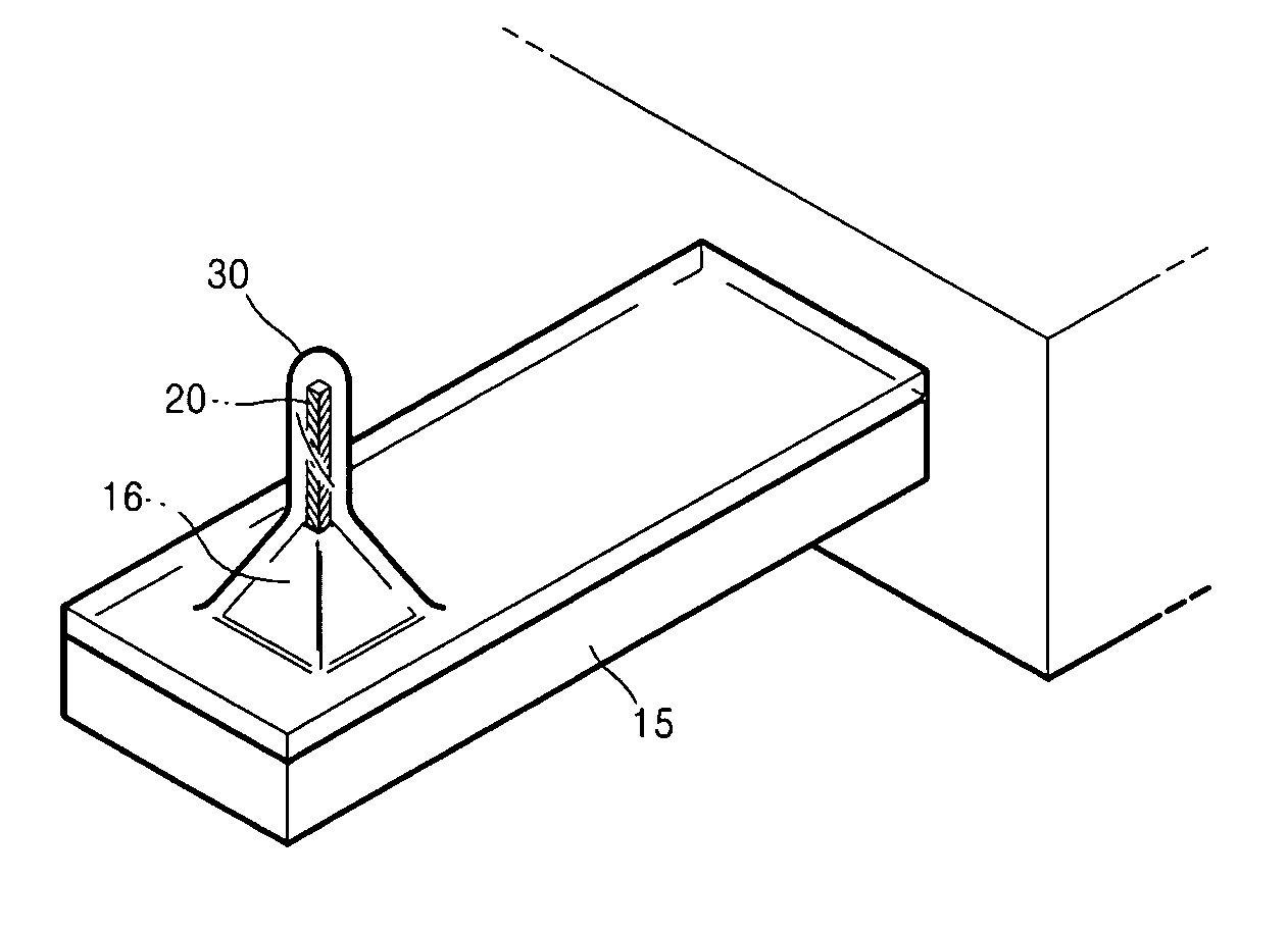
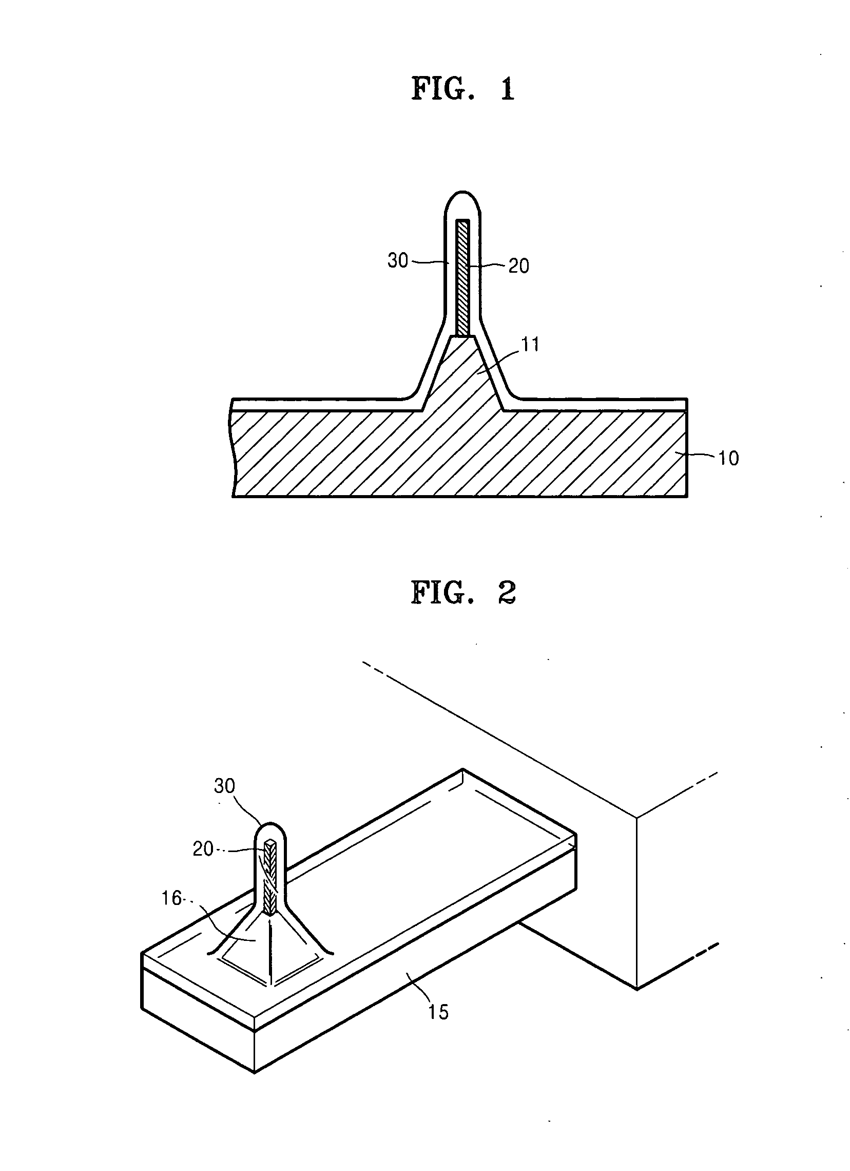
[0026]FIG. 1 is a sectional view of a conductive carbon nanotube according to an embodiment of the present invention.

[0027]Referring to FIG. 1, a carbon nanotube 20 is substantially vertically arranged on a top surface of a substrate 10. That is, a bottom of the carbon nanotube 20 is fixed on the top surface of the substrate 10 to form a carbon nanotube tip. A ruthenium coating layer 30 is formed on the carbon nanotube 20 and extends toward at least a portion of the top surface of the substrate 10.

[0028]The substrate 10 may be a semiconductor substrate or formed of a material such as glass or synthetic resin. However, the substrate 10 is desirably formed of a material that can allow the carbon nanotube 20 and the ruthenium coating laye...


PUM


Abstract

A conductive carbon nanotube tip and a manufacturing method thereof are provided. The conductive carbon nanotube tip includes a carbon nanotube tip substantially vertically placed on a substrate, and a ruthenium coating layer covering a surface of the carbon nanotube tip and extending to at least a part of the substrate. The manufacturing method includes substantially vertically placing a carbon nanotube tip on a substrate, and forming a ruthenium coating layer on the carbon nanotube tip and at least a part of the substrate.

Description

CROSS-REFERENCE TO RELATED PATENT APPLICATION[0001]This application claims the benefit of Korean Patent Application No. 10-2006-0004170, filed on Jan. 14, 2006, in the Korean Intellectual Property Office, the disclosure of which is incorporated herein in its entirety by reference.BACKGROUND OF THE DISCLOSURE[0002]1. Field of the Disclosure[0003]The present disclosure relates to a conductive carbon nanotube tip, a probe having the conductive carbon nanotube tip, and a method of manufacturing the conductive carbon nanotube tip.[0004]2. Description of the Related Art[0005]Generally, a scanning probe microscope (SPM) is a device for measuring a variety of physical values of a test piece by scanning the test piece using a probe. The SPM is referred to as a third generation microscope that is useful for a surface analysis of a thin film.[0006]The SPM includes a probe having a tip and a scanner for scanning a surface of the test piece using the tip, a control / process unit for controlling t...

Claims


Application Information

Patent Timeline
IPC IPC(8): G12B21/02B82B1/00G01Q60/38G01Q60/40G01Q60/46G01Q60/48G01Q70/00G01Q70/12
CPCB82Y15/00B82Y35/00Y10S977/876G01Q70/14Y10S977/879G01Q70/12B26B13/22A61B17/3201A01G3/02A01G2003/023
Inventor CHOI, SANG-JUNLEE, JUNG-HYUNBANG, SANG-BONGSEO, BUM-SEOKLEE, CHANG-SOO
Owner SAMSUNG ELECTRONICS CO LTD
Why Eureka
Try Eureka