Element board for printhead, and printhead having the same

a technology of element boards and printheads, which is applied in the direction of printing, other printing apparatus, etc., can solve the problems of reducing the number of simultaneously drivable heaters, and reducing the number of element boards formed from one wafer. , to achieve the effect of suppressing the cost rise of element boards, signal delay, and increasing resistance and inductan

Inactive Publication Date: 2007-07-19
CANON KK
View PDF11 Cites 12 Cited by
  • Summary
  • Abstract
  • Description
  • Claims
  • Application Information

AI Technical Summary

Benefits of technology

[0034] Hence, the number of element boards formed from one wafer does not greatly decrease even upon an increase in the number of printing elements, suppressing cost rise per element board.
[0035] In a conventional layout, as the wiring line becomes longer, the resistance and inductance increase, and a signal delay and malfunction by noise readily occur. To the contrary, the present invention which shortens the wiring distance of a signal line by arranging at least one of the element selection circuit and the driving selection circuit adjacent to the corresponding driving circuit group, implements high-speed data transfer, and enhances the reliability against malfunction due to signal delay and / or noise.

Problems solved by technology

However, the number of simultaneously drivable heaters is limited because the current supply capability of the power supply is limited, and the voltage drop by the parasitic resistance of a wiring line increases with an increase in current and inhibits supply of desired energy to the heater.
As the number of printing elements (heaters) of the printhead increases for meeting demands for higher image qualities and higher speeds, the following problems arise.
However, as the short side of the rectangular plate-like element board (element substrate) becomes longer, the area of the element board increases, the number of element boards formed from one wafer greatly decreases, and the cost of one element board rises.

Method used


Image

  • Element board for printhead, and printhead having the same
  • Element board for printhead, and printhead having the same
  • Element board for printhead, and printhead having the same

Examples


first embodiment

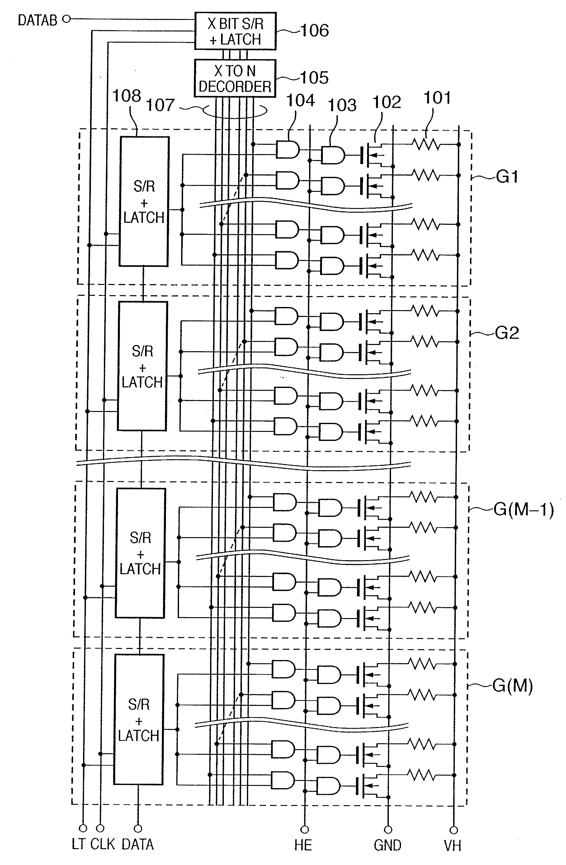
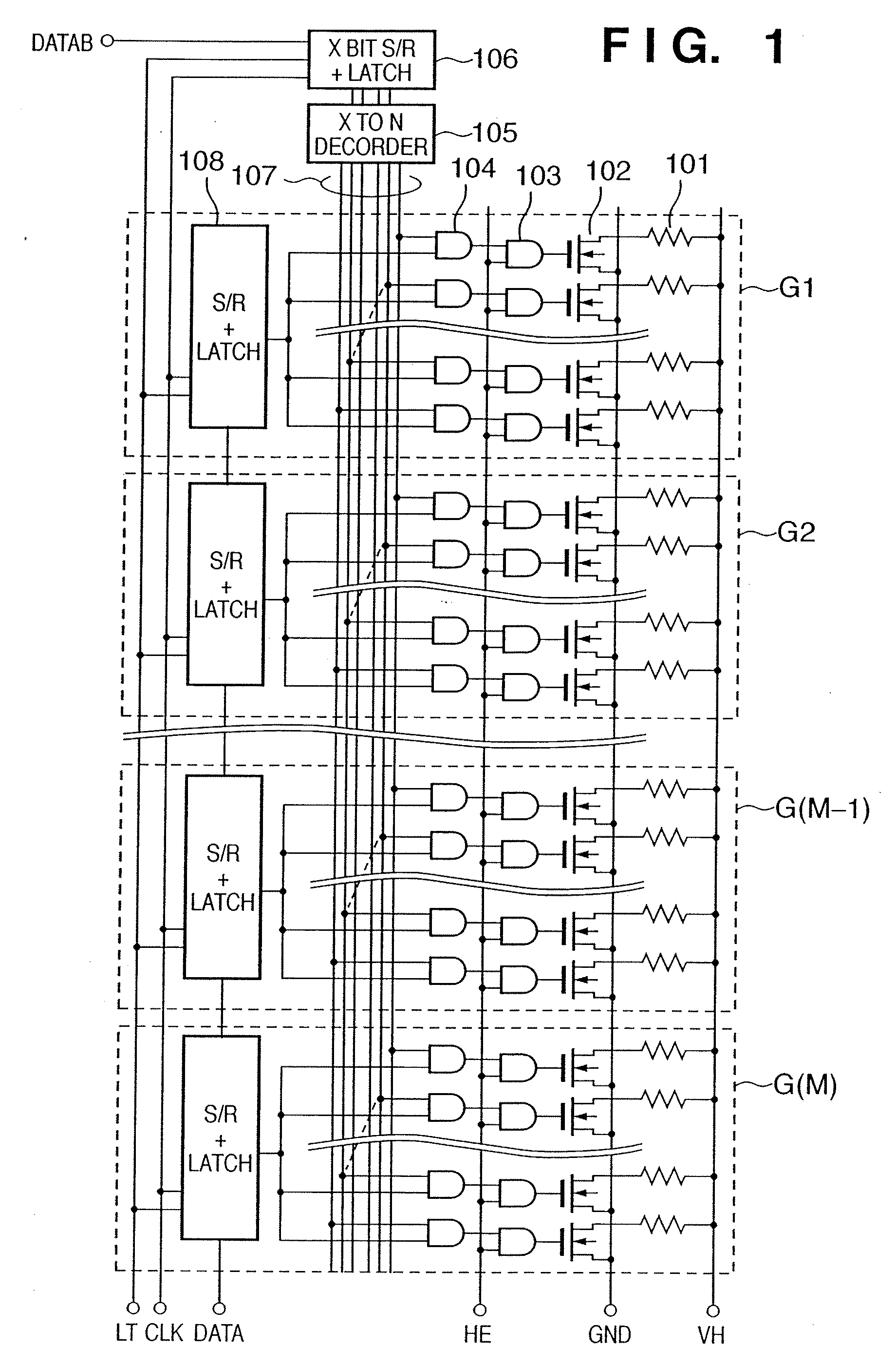
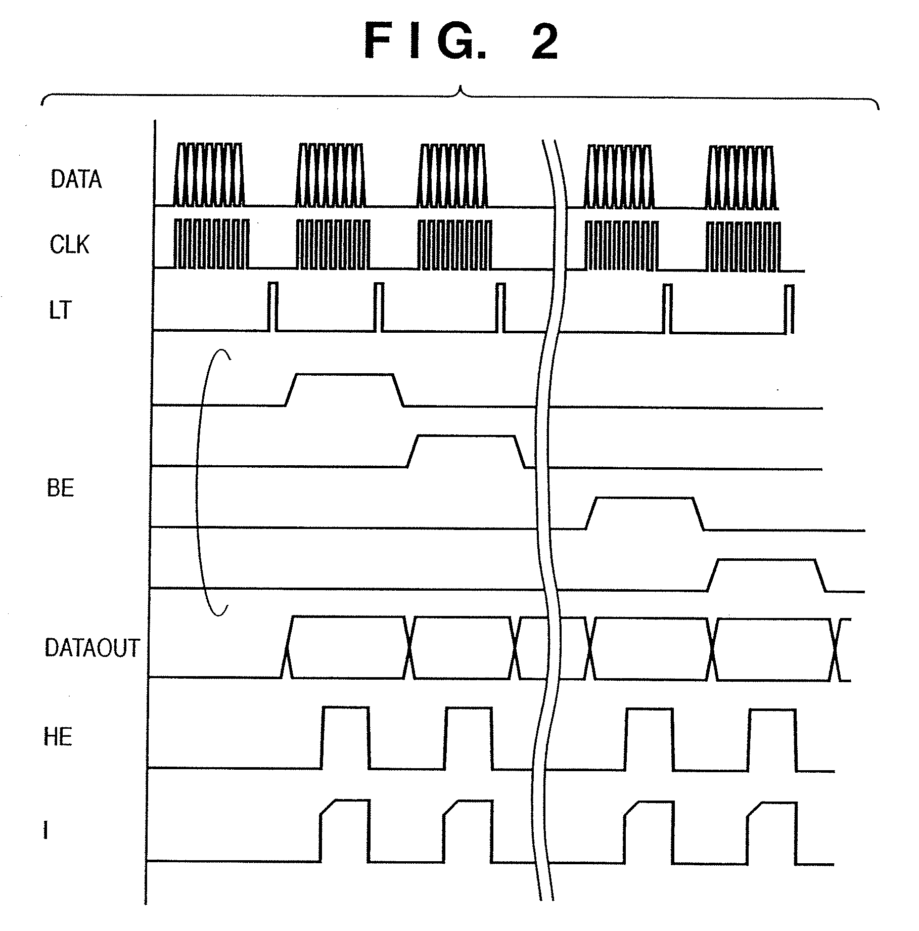
[0089] The first embodiment of a printhead according to the present invention will be described.FIG. 1 is a circuit diagram showing a printhead which performs matrix driving of selecting an arbitrary heater on the basis of the ANDs between outputs from registers for storing M data and block selection signals which are N decoder signal outputs so as to drive M×N heaters for M heaters N times in time division. Elements are built in an element board.

[0090] In FIG. 1, reference numerals 101 denote heaters serving as printing elements; 102, transistors which drive the respective heaters; 103 and 104, AND circuits which AND logical signal inputs; 105, an X to N decoder which decodes an X-bit block control signal supplied from a printer main body and selects one of N block selection lines; and 106, a shift register+latch circuit which stores, in synchronism with a CLK signal, the block control signal serially transferred from the printer main body and latches the block control signal by a...

second embodiment

[0112] The second embodiment of a printhead according to the present invention will be described. In the following description, a description of the same parts as those in the first embodiment will be omitted, and characteristic parts of the second embodiment will be mainly explained.

[0113] The circuit of the printhead according to the second embodiment is the same as that according to the first embodiment shown in FIG. 1. The second embodiment is different from the first embodiment in the layout on the element board.

[0114]FIG. 4 is a view showing an actual layout on an element board according to the second embodiment, similar to FIG. 3. In the layout of the first embodiment shown in FIG. 3, the length in the heater array direction in each group and the length in the long-side direction of a corresponding driving circuit are set equal to each other. In the layout of the second embodiment, the length in the long-side direction of a corresponding driving circuit can be set smaller t...

third embodiment

[0119] The third embodiment of a printhead according to the present invention will be described. In the following description, a description of the same parts as those in the first and second embodiments will be omitted, and characteristic parts of the third embodiment will be mainly explained.

[0120]FIG. 5 is a circuit diagram showing the third embodiment in which decoder circuits 501 are arranged in correspondence with respective heaters. In the first embodiment of FIG. 1, the X to N decoder circuit 105 is arranged commonly to M groups each having N heaters. N block selection lines are connected to AND circuits in each group in accordance with an output from the decoder circuit 105, and an arbitrary heater within the group is selected. To the contrary, in FIG. 5, X block control lines 502 are connected to the decoder circuits 501 arranged for respective heaters within each group in accordance with an output from an X-bit shift register 106, and a heater within the group is selecte...


PUM


Abstract

In a printhead element board including a plurality of printing elements which align in a predetermined direction, driving circuits which drive the printing elements, and an element selection circuit which selects printing elements within each group for each group having a predetermined number of adjacent printing elements, a plurality of element selection circuits are laid out adjacent to the driving circuits of the respective groups. With this layout, even if the number of printing elements increases, only the length in the printing element array direction increases without increasing the length in a direction perpendicular to the printing element array direction.

Description

FIELD OF THE INVENTION [0001] The present invention relates to an element board for a printhead and a printhead having the same and, more particularly, to the layout of an element board for a printhead on which a plurality of printing elements that align in a predetermined direction and divided into a plurality of groups for a predetermined number of printing elements, and a driving circuit for driving the printing elements are formed on the same element board. BACKGROUND OF THE INVENTION [0002] As an information output apparatus in a wordprocessor, personal computer, facsimile apparatus, and the like, a printing apparatus which prints information such as a desired character or image on a sheet-like printing medium such as a paper sheet or film widely adopts a serial printing method of printing by reciprocal scanning in a direction perpendicular to the feed direction of a printing medium such as a paper sheet because this method can achieve cost reduction and easy downsizing. [0003]...

Claims


Application Information

Patent Timeline
Patent Type & Authority Applications(United States)
IPC IPC(8): B41J29/38B41J2/01B41J2/05B41J2/14
CPCB41J2/04541B41J2/0458B41J2/04543B41J2/01B41J2/05
Inventor HIRAYAMA, NOBUYUKIKASAI, RYOSAKURAI, MASATAKA
Owner CANON KK
Why Eureka
Try Eureka