Sensor package substrate, sensor module including the same, and electronic component embedded substrate

a technology for sensors and substrates, applied in the direction of instruments, fluid pressure measurement, heat measurement, etc., can solve the problems of increasing etc., and achieve the effect of reducing the distance of the wiring and reducing the area of the substra

Active Publication Date: 2020-05-21
TDK CORPARATION
View PDF0 Cites 2 Cited by
  • Summary
  • Abstract
  • Description
  • Claims
  • Application Information

AI Technical Summary

Benefits of technology

[0004]It is therefore an object of the present invention to provide a sensor package substrate allowing a reduction in the distance of the wirings connecting the sensor chip and other electronic components, a sensor module having the sensor package substrate, and an electronic component embedded substrate.
[0005]Another object of the present invention is therefore to provide a sensor package substrate allowing a reduction in the substrate area, a sensor module having the sensor package substrate, and an electronic component embedded substrate.
[0008]According to the present invention, the sensor chip and the electronic component are laid out so as to overlap each other, so that by reducing the thickness of an insulating layer interposed between the sensor chip and the electronic component, it is possible not only to reduce the distance of a wiring for sensor chip and electronic component, but also to reduce the area of the substrate. Further, the sensor chip can detect the physical quantity of a measurement target through the through hole.
[0011]In the present invention, the electronic component may be embedded in the substrate. This eliminates the need to mount the electronic component on the other side of the substrate opposite to the one side thereof on which the sensor chip is mounted, thereby allowing the other side to be brought closer to a mother board, which can enhance the sensitivity of the sensor.
[0012]The sensor package substrate according to the present invention may further include a metal film positioned inside the through hole and having an opening smaller in diameter than the through hole. This can prevent electrostatic breakdown of the sensor chip and make dust or the like unlikely to adhere to the sensor chip through the through hole.
[0015]As described above, according to the present invention, in the sensor package substrate, sensor module having the same, and electronic component embedded substrate, it is possible to reduce the distance of a wiring for connecting the sensor chip and the electronic component and to reduce the area of the substrate.

Problems solved by technology

However, in the sensor module described in JP 2013-149792 A, the sensor chip and other electronic components are mounted on the same plane, so that it is difficult to reduce the distance of the wirings connecting the senor chip and the other electronic component, which in turn results in an increase in the substrate area.

Method used


Image

  • Sensor package substrate, sensor module including the same, and electronic component embedded substrate
  • Sensor package substrate, sensor module including the same, and electronic component embedded substrate
  • Sensor package substrate, sensor module including the same, and electronic component embedded substrate

Examples


Embodiment Construction

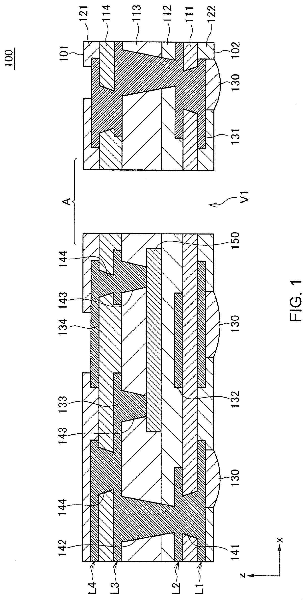
[0041]Hereinafter, preferred embodiments of the present invention will be described in detail with reference to the accompanying drawings. Positional relationships such as upper, lower, left, and right will be based on those in the drawings unless otherwise noted. Further, the dimensional proportions in the drawings are not limited to those illustrated in the drawings. The following embodiments are merely illustrative purposes only, and the invention is not limited to the following embodiments. Further, the present invention can be variously modified without departing from the gist of the invention.

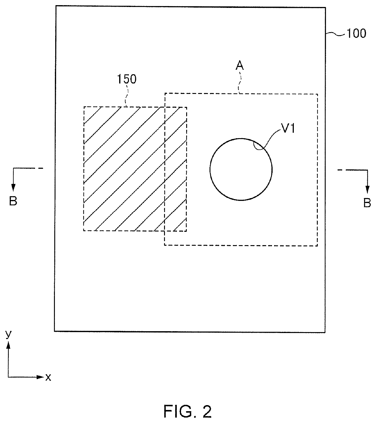
[0042]FIG. 1 is a schematic cross-sectional view for explaining the structure of a sensor package substrate 100 according to one embodiment of the present invention. FIG. 2 is a schematic plan view of the sensor package substrate 100. The cross section illustrated in FIG. 1 is a cross section taken along line B-B in FIG. 2.

[0043]As illustrated in FIGS. 1 and 2, the sensor package substrat...


PUM

PropertyMeasurementUnit
thicknessaaaaaaaaaa
thicknessaaaaaaaaaa
thicknessaaaaaaaaaa

Abstract

A sensor package substrate disclosed in the present specification has a mounting area in which a sensor chip is mounted and a controller chip connected to the sensor chip. A through hole is formed in the sensor package substrate so as to overlap the mounting area in a plan view and to penetrate the substrate from one surface to the other surface thereof. The mounting area and the controller chip overlap each other in a plan view. According to the present invention, by reducing the thickness of an insulating layer, it is possible not only to reduce the distance of a wiring for the sensor chip and controller chip, but also to reduce the area of the substrate.

Description

BACKGROUND OF THE INVENTIONField of the Invention[0001]The present invention relates to a sensor package substrate and a sensor module having the same and, more particularly, to a sensor package substrate for mounting a sensor that detects air vibration, air pressure, air temperature or air composition, and a sensor module having the same. The present invention relates also to an electric component embedded substrate suitable as the sensor package substrate.Description of Related Art[0002]As a sensor module having a sensor chip such as a temperature sensor, a sensor module described in JP 2013-149792 A is known. The sensor modules described in JP 2013-149792 A is formed as follows: first, a sensor chip and other electronic components are accommodated in a plurality of recessed parts formed in a substrate; then, wirings for connecting the sensor chip and the electronic components are formed; and finally, the surface of the substrate is resin-sealed.[0003]However, in the sensor module...

Claims


Application Information

Patent Timeline
Patent Type & Authority Applications(United States)
IPC IPC(8): H01L23/13H01L25/18H01L23/538G01L9/00G01H3/00G01K13/02G01N33/00
CPCG01K2013/024G01K13/02G01N33/0027H01L25/18H01L23/13G01H3/00G01L9/0041H01L23/5389H01L2224/04105H01L2224/73267H01L2224/32225H01L2224/92244H01L2224/48227H01L2924/15311H01L2924/15151H01L2224/73265H01L2224/24226H01L24/19H01L24/48H01L24/73H01L24/32H01L24/92H01L2224/16227H01L2924/1815H01L24/16H01L2924/00012H01L2924/00
Inventor TSUYUTANI, KAZUTOSHISUZUKI, YOSHIHIROMOTOHASHI, AKIRA
Owner TDK CORPARATION
Why Eureka
Try Eureka