Inductor module, silicon tuner module and semiconductor device

a technology of silicon tuner module and semiconductor device, which is applied in the direction of transformer/inductance coil/winding/connection, transformer/react mounting/support/suspension, electrical apparatus construction details, etc., can solve the problem of lowering the characteristics of the inductor under the influence of undesired radiation, suppressing the adverse effects of parasitic resistance, suppressing the degradation of inductor characteristics,

Inactive Publication Date: 2012-12-25
SONY CORP
View PDF9 Cites 2 Cited by
  • Summary
  • Abstract
  • Description
  • Claims
  • Application Information

AI Technical Summary

Benefits of technology

[0011]However, when simple shortening of the laying-around distances of wiring and the like is merely adopted, there would arise a problem in that inductor characteristics are lowered under influences of undesired radiation from the ICs. Specifically, although the shortening of the laying-around distances of wiring and the like can restrain the adverse effects of parasitic resistance, parasitic capacitance, parasitic inductance, etc., it results in that the inductor formed to function as a filter is located closer to the IC. Therefore, the inductance is more likely to be influenced by radiation of harmonic components generated from a circuit called a voltage-controlled oscillator (VCO) integrated in the IC, and the inductor characteristics are degraded by the influence of radiation of harmonics (unwanted radiation).
[0012]Thus, there is a need for provision of an inductor module, a silicon tuner module and a semiconductor device which can contribute to suppression of adverse effects of unwanted radiation from an IC, while making it possible to suppress the adverse influences of parasitic resistance, parasitic capacitance, parasitic inductance, etc. by shortening the laying-around distances of wiring and the like, in the case where an inductor functioning as a filter is provided in a module separately from the functions integrated in an IC.
[0015]In addition, notwithstanding the inductor is formed at such a position as to overlap with the IC mounting part on a plan-view basis, the magnetic body is present intermediately between the IC mounting part and the inductor and, therefore, unwanted radiation from the IC mounted on the IC mounting part is absorbed by an electromagnetic wave absorbing action of the magnetic body. Consequently, bad influences of the unwanted radiation are restrained from being exerted on the inductor. Moreover, since the body present intermediately between the IC mounting part and the inductor is a magnetic body, an L value amplifying action of the magnetic body on the inductor can also be expected.
[0016]The L value amplifying action and the electromagnetic wave absorbing action of the magnetic body are displayed through utilization of characteristics of the real part (μ′) and the imaginary part (μ″) of the permeability of the magnetic body. To be more specific, in the frequency band used for the IC, the L value amplifying action is displayed through utilization of the μ′ characteristic of the magnetic body, whereas in the frequency band in which unwanted radiation from the IC might produce a problem, the electromagnetic wave absorbing action is displayed through utilization of the μ″ characteristic of the magnetic body. Besides, the use of a body including a magnetic material selected from among a NiZn ferrite, a NiZnCu ferrite and a Ba ferrite as the magnetic body makes it possible to utilize the μ′ characteristic in the frequency band used for the IC and to utilize the μ″ characteristic in the frequency band in which the unwanted radiation might produce a problem.
[0017]According to the embodiments of the present invention, the laying-around distances of wiring and the like for securing connection between the IC (e.g., silicon tuner IC) mounted on the IC mounting part and the inductor formed in the substrate can be shortened, so that it is possible to suppress the adverse effects of parasitic resistance, parasitic capacitance, parasitic inductance, etc. As a result, it is possible to realize suppression of degradation of inductor characteristics. Furthermore, bad influences of unwanted radiation from the ICs mounted on the IC mounting part can be restrained from being exerted on the inductor, by the simple configuration in which the magnetic body including a magnetic material selected from among a NiZn ferrite, a NiZnCu ferrite and a Ba ferrite is intermediately provided between the IC mounting part and the inductor. Thus, the configuration according to an embodiment of the present invention can contribute to suppression of adverse effects of the unwanted radiation from the ICs, even in the case where the laying-around distances of wiring and the like are shortened.

Problems solved by technology

However, when simple shortening of the laying-around distances of wiring and the like is merely adopted, there would arise a problem in that inductor characteristics are lowered under influences of undesired radiation from the ICs.

Method used


Image

  • Inductor module, silicon tuner module and semiconductor device
  • Inductor module, silicon tuner module and semiconductor device
  • Inductor module, silicon tuner module and semiconductor device

Examples


Embodiment Construction

[0021]Now, an inductor module, a silicon tuner module and a semiconductor device according to embodiments of the present invention will be described below, referring to the drawings.

[0022]First of all, the configuration of the silicon tuner module serving as a specific example of the semiconductor device will be described.

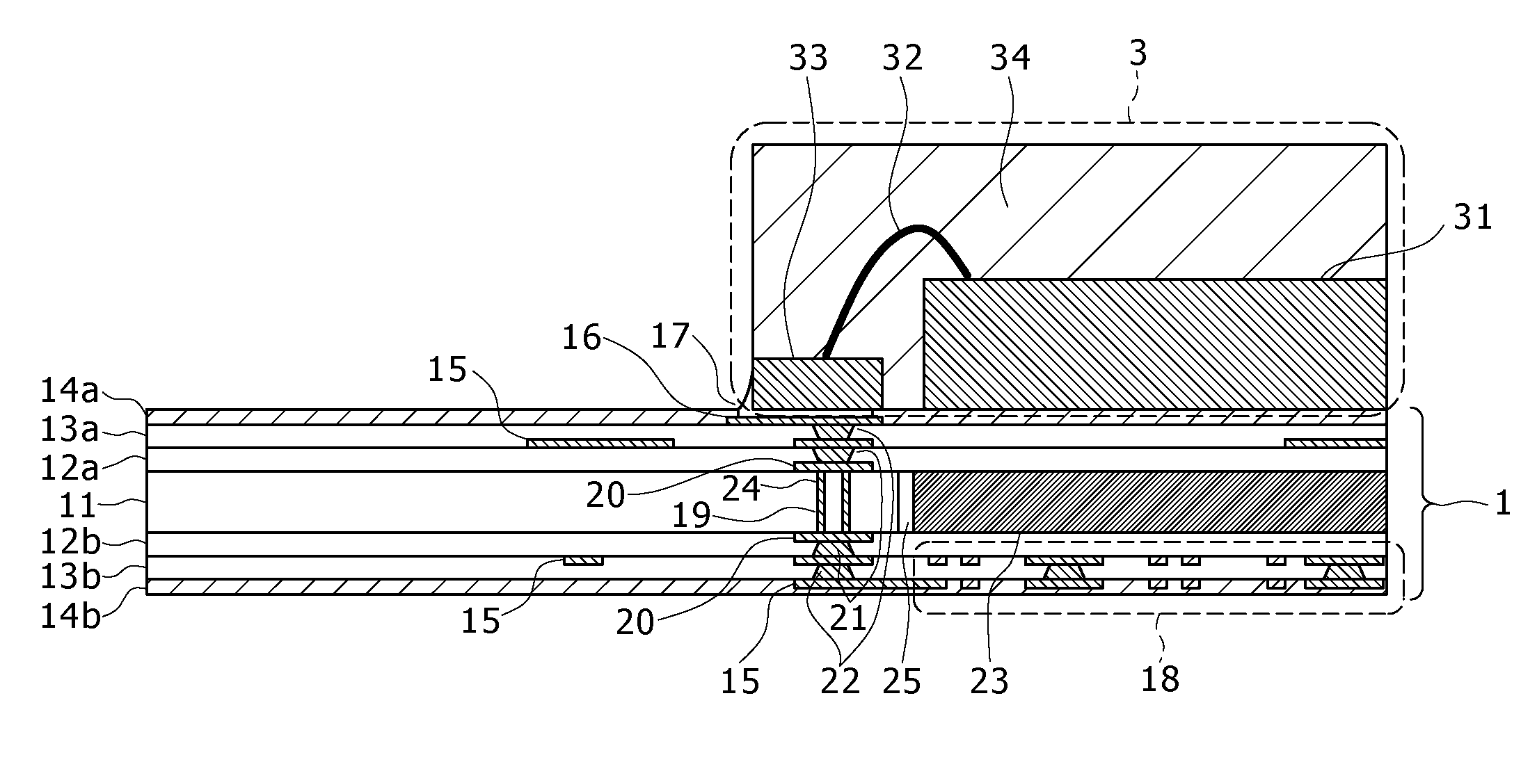
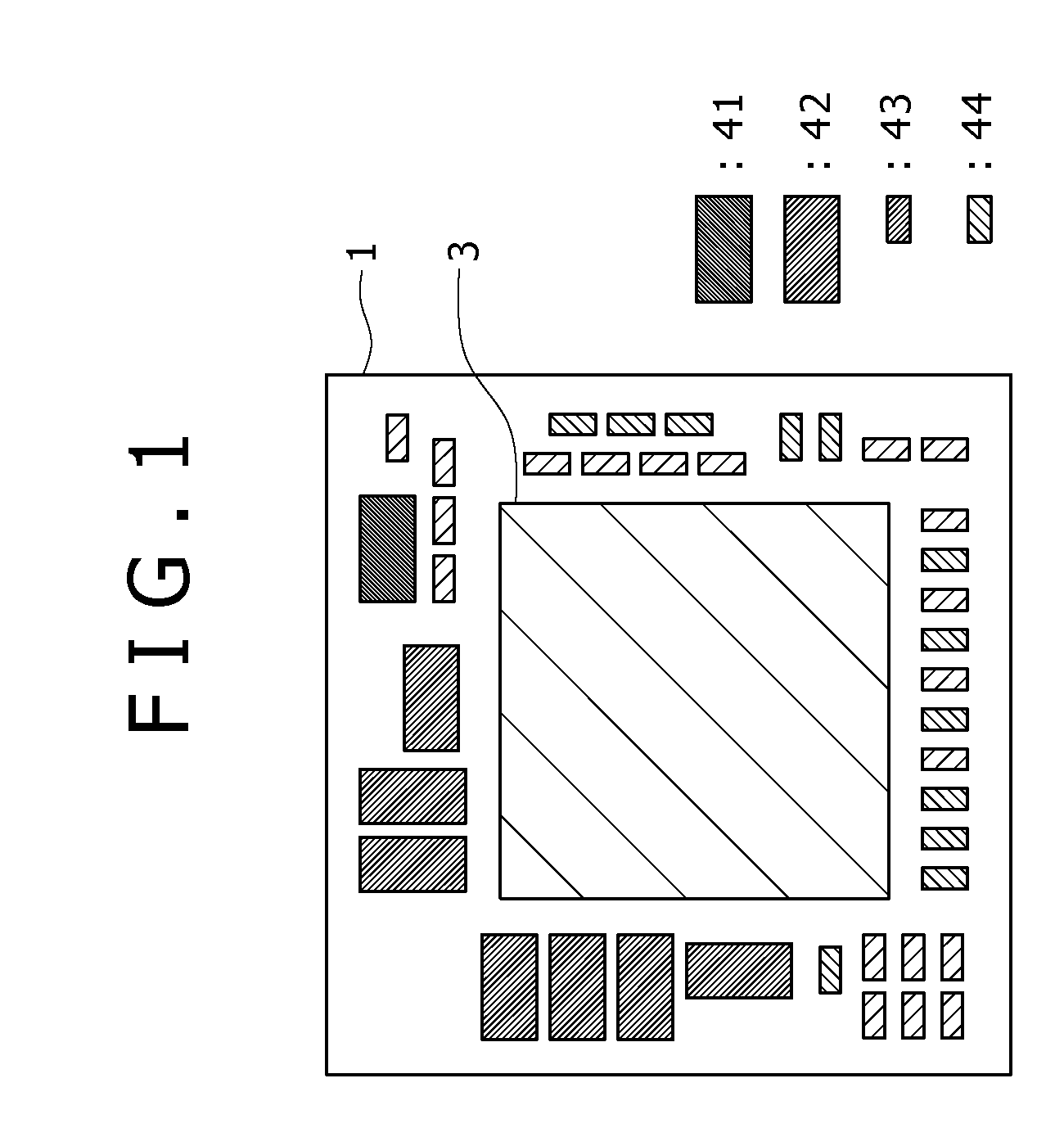
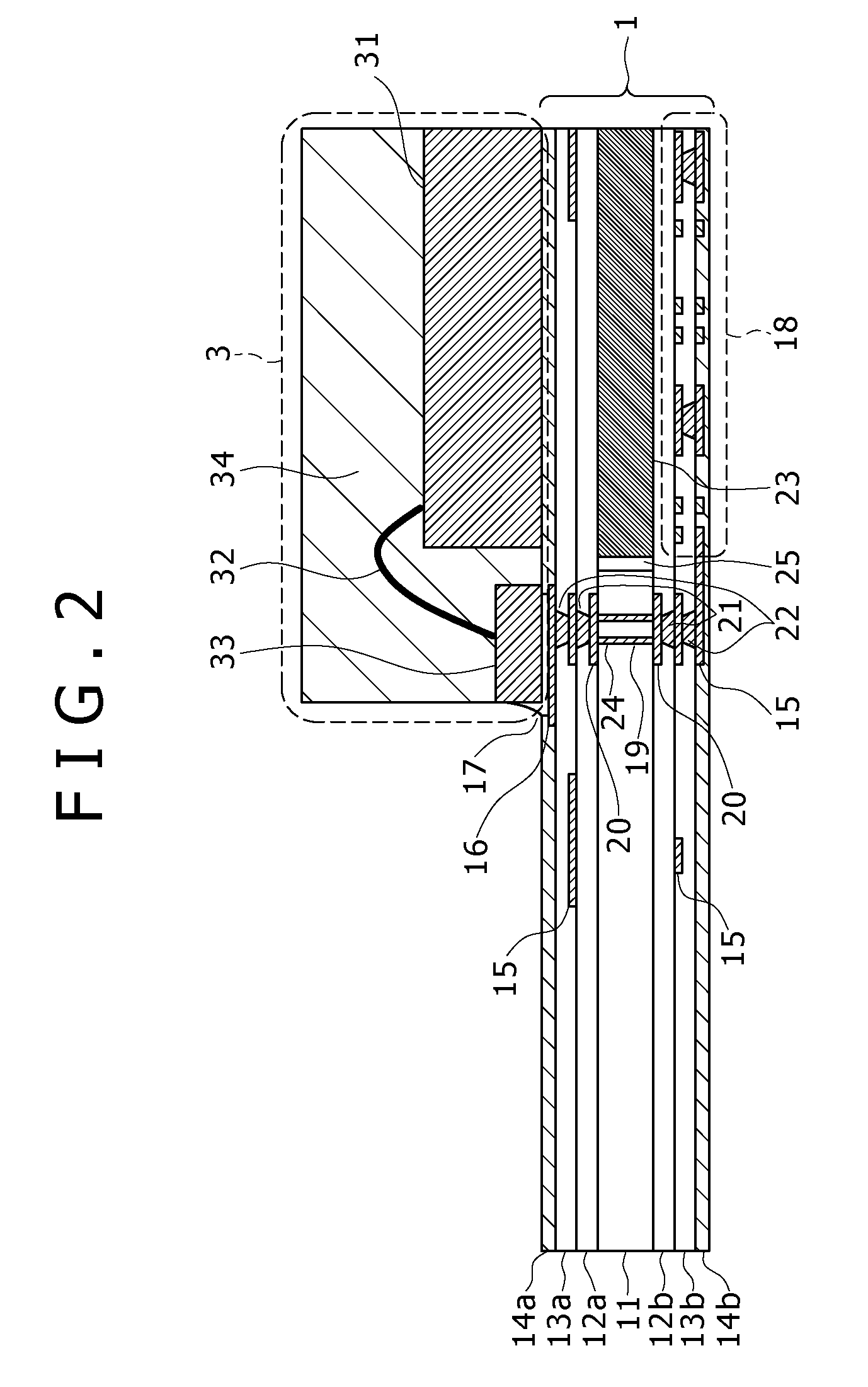
[0023]FIG. 1 is a plan diagram schematically showing the general configuration of the silicon tuner module, and FIG. 2 is a side sectional view showing a configuration example of a major part of the same.

[0024]The silicon tuner module is for use in the state of being mounted in a television receiver, realizing a function of receiving television broadcasts.

[0025]For this purpose, the silicon tuner module includes a silicon tuner IC 3 mounted on a substrate 1, as shown in FIG. 1. Incidentally, on the substrate 1, passive component parts such as a balance-unbalance converter 41, which is an element for conversion of electrical signals being in a balanced state and an ...


PUM

PropertyMeasurementUnit
frequenciesaaaaaaaaaa
frequencyaaaaaaaaaa
permeabilityaaaaaaaaaa

Abstract

Disclosed herein is an inductor module including a substrate functioning as a printed wiring board or an interposer; an IC mounting part formed on a surface of the substrate; an inductor which is formed in the substrate at such a position as to overlap with the IC mounting part on a plan-view basis and which is connected to an IC mounted on the IC mounting part; and a magnetic body including a magnetic material selected from among a NiZn ferrite, a NiZnCu ferrite and a Ba ferrite, the magnetic body being disposed intermediately between the IC mounting part and the inductor.

Description

BACKGROUND OF THE INVENTION[0001]1. Field of the Invention[0002]The present invention relates to an inductor module, a silicon tuner module and a semiconductor device.[0003]2. Description of the Related Art[0004]In recent years, with the advent of organic electroluminescence (EL) television sets, extra-thin liquid crystal display (LCD) television sets and the like, there is a need for more reductions in the size and thickness of the tuner module, which is one of the largest functional parts in television receivers. In addition, increases in the number of functions such as incorporation of a recording function and a multi-window display mode have been being made, and there are an increasing number of cases where a plurality of tuner modules are mounted in a single television receiver. From this point of view, also, there has been a keener need for smaller-sized tuner modules.[0005]To meet such a need as above, recently, there has been vigorous development of silicon tuner modules in ...

Claims


Application Information

Patent Timeline
Patent Type & Authority Patents(United States)
IPC IPC(8): H01F27/06H01L21/12H01F27/30
CPCH01L23/552H01L23/645H01L25/16H01L2224/48091H01L2924/01078H01L2924/01079H01L2924/14H01L2924/19041H01L2924/30107H01L2924/3011H01L2924/3025H01L2924/00014H01L24/48H01L2224/45147H01L2924/00H01L24/45H01L2924/181H01L2224/45099H01L2224/05599H01L2924/00011H01L2924/00012
Inventor OKA, SHUICHIMATSUMOTO, KATSUJIYANAGAWA, SHUSAKU
Owner SONY CORP
Why Eureka
Try Eureka