

Organic electroluminescent device
- Summary
- Abstract
- Description
- Claims
- Application Information
AI Technical Summary
Benefits of technology
Problems solved by technology
Method used
Image

Examples
examples
[0048] Next, manufacturing procedures of each of organic electroluminescent devices of concrete Example according to an embodiment of the invention and Comparative Examples 1 and 2 against this Example are described.
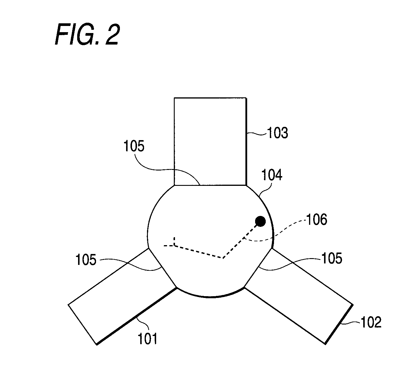
[0049] Incidentally, a vacuum device as illustrated in FIG. 2 was used in the preparation of each of organic electroluminescent devices of the Example and Comparative Examples. A vacuum device 100 as illustrate in FIG. 2 is provided with a vapor deposition compartment 101, a sputtering compartment 102, a glove box compartment 103, and a carrier compartment 104 connected to each of them. A door 105 is provided between the carrier compartment 104 and each of the compartments 101 to 103 for the purpose of isolating a gas atmosphere in the inside thereof. A robot arm 106 is set up within the carrier 104 for the purpose of carrying a treating substrate into each of the compartments 101 to 103 via the carrier compartment 104. Thus, in the vacuum device 100, the treatment can ...
PUM
 Abstract
Description
Claims
Application Information