Group lll nitride semiconductor light-emitting device

Inactive Publication Date: 2011-10-06
TOYODA GOSEI CO LTD
View PDF2 Cites 33 Cited by
  • Summary
  • Abstract
  • Description
  • Claims
  • Application Information

AI Technical Summary

Benefits of technology

[0007]The present invention has been accomplished for solving such a problem. An object of the present invention is to improve emission performance

Problems solved by technology

In addition, since the AlGaN layer acts as a barrier against electrons, resistance to electrons is not reduced, and confinement of holes in the light-emitting layer is not improved.
In the device disclosed in Japanese Patent Application Laid-Open (kokai) No. 2007-180499, the light-emit

Method used


Image

  • Group lll nitride semiconductor light-emitting device
  • Group lll nitride semiconductor light-emitting device
  • Group lll nitride semiconductor light-emitting device

Examples


Example

Embodiment 1

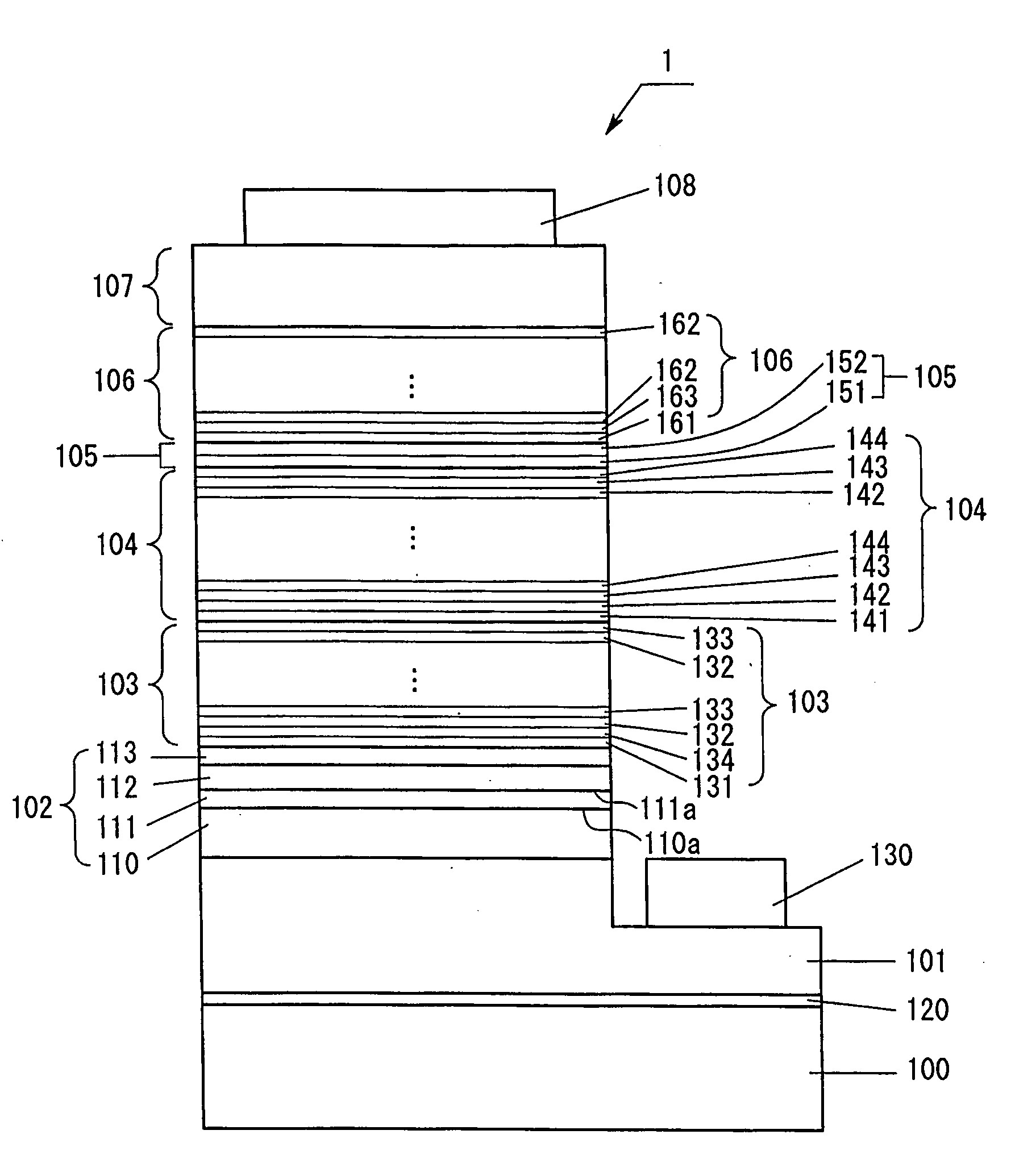
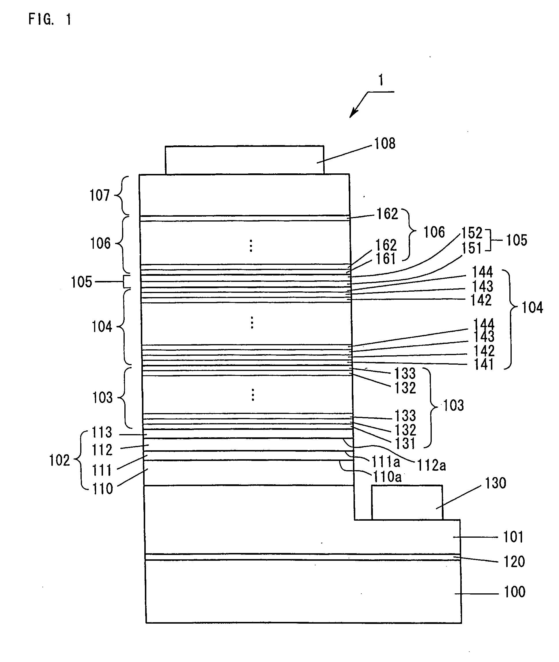
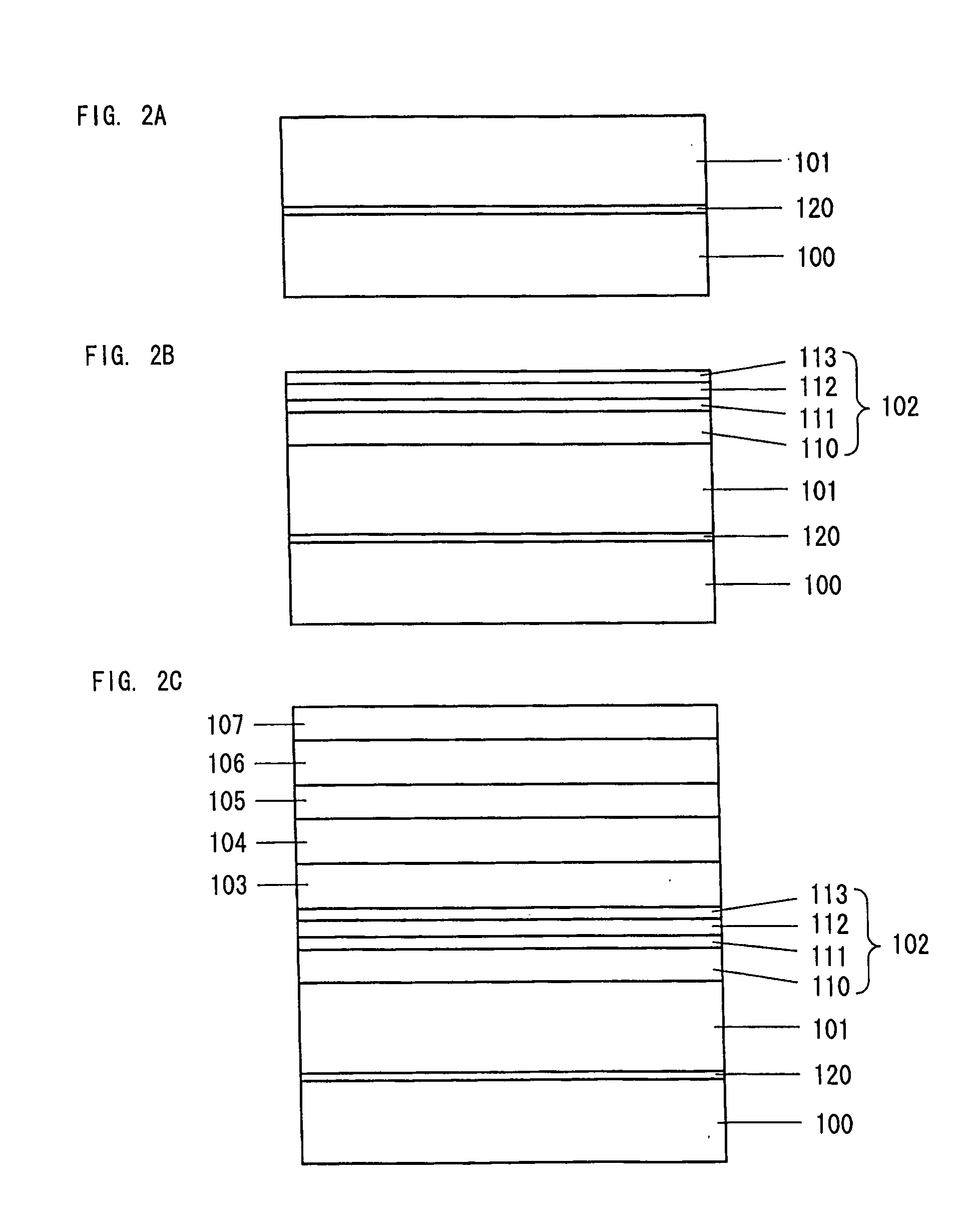
[0027]FIG. 1 shows the configuration of a light-emitting device 1 according to Embodiment 1. The light-emitting device 1 has a structure including a sapphire substrate 100; an AlN buffer layer 120; an n-type contact layer 101, an ESD layer 102, an n-type-layer-side cladding layer (referred to as “n-type cladding layer” throughout the Embodiments) 103, a light-emitting layer 104, an undoped cladding layer 105, a p-type-layer-side cladding layer (referred to as “p-type cladding layer” throughout the Embodiments) 106, and a p-type contact layer 107, the layers 101 to 107 being formed of a Group III nitride semiconductor and deposited on the substrate 100 via the buffer layer 120; a p-electrode 108 formed on the p-type contact layer 107; and an n-electrode 130 formed on a portion of the n-type contact layer 101 exposed through removal of the corresponding portions of the layers 102 to 107 by etching from the p-type contact layer 107.

[0028]The surface of the sapphire substrat...

Example

Embodiment 2

[0055]As shown in FIGS. 4 and 5, the light-emitting device according to the present embodiment has the same configuration as the light-emitting device according to Embodiment 1, except that the n-type cladding layer 103 includes an undoped GaN layer 134 (thickness: 1 nm) interposed between the undoped In0.077Ga0.923N layer 131 and the undoped Al0.2Ga0.8N layer 132. When the Al0.2Ga0.8N layer 132 is grown directly on the In0.077Ga0.923N layer 131, the difference in lattice constant between these two layers increases, and crystal defects may be generated at the interface between the In0.077Ga0.923N layer 131 and the Al0.2Ga0.8N layer 132. In addition, since raw material gases employed for growth of the In0.077Ga0.923N layer 131 remain in the piping or the crystal growth apparatus, an AlxGa1-x-yInyN (0131 and 132. The thus-formed layer may deteriorate characteristics, and may prevent formation of a sharp band structure. In order to avoid such problems, the undoped GaN layer...


PUM


Abstract

The present invention provides a Group III nitride semiconductor light-emitting device exhibiting improved emission performance without increasing driving voltage. The Group III nitride semiconductor light-emitting device includes at least an n-type-layer-side cladding layer, a light-emitting layer, and a p-type-layer-side cladding layer, each of the layers being formed of a Group III nitride semiconductor. The n-type-layer-side cladding layer is a superlattice layer having a periodic structure including an InyGa1-yN (0<y<1) layer, an AlxGa1-xN (0<x<1) layer, and a GaN layer. The AlxGa1-xN (0<x<1) layer has such a thickness that electrons tunnel through the AlxGa1-xN layer and holes are confined in the light-emitting layer.

Description

BACKGROUND OF THE INVENTION[0001]1. Field of the Invention[0002]The present invention relates to a Group III nitride semiconductor light-emitting device which suppresses an increase in driving voltage and which exhibits improved emission performance.[0003]2. Background Art[0004]Hitherto, various known Group III nitride semiconductor light-emitting devices are known, and some of them are disclosed in Japanese Patent Application Laid-Open (kokai) Nos. H11-191639 and 2007-180499. Japanese Patent Application Laid-Open (kokai) No. H11-191639 discloses a Group III nitride semiconductor light-emitting device having a structure in which a light-emitting layer is stacked on n-type layers; i.e., a third layer bonded to the light-emitting layer, a second layer bonded to the third layer, and a first layer bonded to the second layer. The second layer has a superlattice structure formed of two layers (AlGaN layer and GaN layer) or a superlattice structure formed of two layers (AlGaN layer and InG...

Claims


Application Information

Patent Timeline
IPC IPC(8): H01L33/04
CPCH01L33/04H01L33/06H01L33/32
Inventor OKUNO, KOJIMIYAZAKI, ATSUSHI
Owner TOYODA GOSEI CO LTD
Why Eureka
Try Eureka