Electron buffering materials, electron transport materials and organic electroluminescent device comprising the same
Active Publication Date: 2018-11-08
ROHM & HAAS ELECTRONIC MATERIALS LLC
View PDF0 Cites 2 Cited by
Summary
Abstract
Description
Claims
Application Information
AI Technical Summary
This helps you quickly interpret patents by identifying the three key elements:
Problems solved by technology
Method used
Benefits of technology
Benefits of technology
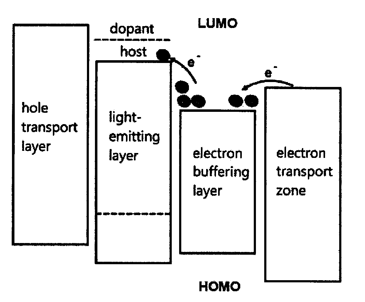
This patent discusses the use of a special material called an electron buffering material or electron transport material in organic electroluminescent devices. This material helps to control electron injection and improves the connection between the light-emitting layer and electron injection layer, resulting in devices with better brightness and efficiency. By using a combination of this material and another material called an electron buffering layer, devices can have low driving voltage, high efficiency, and long lifespan. Overall, this patent explains a way to improve the performance of organic electroluminescent devices.
Problems solved by technology
However, a phosphorous material for emitting blue light has the following disadvantages, which are blocking realization of full color display: roll-off is reduced at high current due to loss of excessively formed excitons, thereby deteriorating performances; the blue-emitting phosphorescent material itself has a problem in long term stability of lifespan; and color purity is rapidly decreasing by lapse of time.
A fluorescent material has been used, but has several problems.
First, when exposed to high-temperature during a panel production process, a current feature can be changed, which can cause a change in luminance.
Furthermore, due to a structural characteristic, an interface feature between a light-emitting layer and an electron injection layer can deteriorate, which can cause a decrease of luminance.
However, the proposed combination makes holes become greatly trapped, which can cause light-emitting sites in a light-emitting layer to shift to the side close to a hole transport layer, thereby light being emitted at an interface.
The light-emission at an interface decreases lifespan of a device, and efficiencies are not satisfactory.
It is not easy to solve the aforementioned problems of a fluorescent material by improvement of a light-emitting material itself.
However, this Korean patent reference fails to disclose an organic electroluminescent device employing a compound having a phenanthrothiazole skeleton in an electron buffering layer or an electron transport layer.
However, in this Japanese reference, groups of the electron buffering materials are limited to Alq3 derivatives, and it is desired to restrictelectron mobility.
Thus the improvement in efficiency and lifespan is limited.
However, this Korean patent reference fails to disclose the compounds having a phenanthrothiazole skeleton, and according to this Korean patent reference, the optimization of an organic electroluminescent device comprising an electron buffering layer or an electron transport layer is limited.
Method used
Image
Click on the blue label to locate the original text in one second.
Reading with bidirectional positioning of images and text.
[0120]After adding compound A (CAS: 1044146-16-8, 36 g, 124 mmol), 4-chloro-2-formylbenzene boronic acid (25.2 g, 136 mmol), tetrakis(triphenylphosphine)palladium (5.7 g, 5.0 mmol), sodiumcarbonate (33 g, 150 mmol), toluene (600 mL), EtOH (150 mL), and distilled water (150 mL) into a reaction vessel, the mixture was stirred at 140° C. for 3 hours. After completion of the reaction, the precipitated solid was washed with distilled water and MeOH. The obtained compound 1-1 was used in the next reaction without further purification.
[0121]2) Preparation of Compound 1-2
[0122]After introducing compound 1-1 (45.6 g, 130 mmol), (methoxymethyl)triphenylphosphonium chloride (74.3 g, 217 mmol), and tetrahydrofuran (1500 mL) into a reaction vessel, the reaction mixture was stirred for 5 minutes, and then potassium tert-butoxide (KOtBu) (1M in THF, 220 mL) was slowly added dropwise thereto at 0° C. The mixture was ...
[0129]After adding compound C (10 g, 29 mmol), bis(pinacolato)diborane (8.8 g, 34.8 mmol), tris(dibenzylideneacetone)dipalladium (Pd2(dba)3) (1.3 g, 1.45 mmol), 2-dicyclohexylphosphino-2′,6′-dimethoxybiphenyl(s-phos) (1.2 g, 2.9 mmol), potassium acetate (KOAc) (8.5 g, 87 mmol), and 1,4-dioxane (150 mL) into a reaction vessel, the mixture was then stirred at 140° C. for 3 hours. After completion of the reaction, the mixture was cooled to room temperature, and then was extracted with ethyl acetate. After the extracted organic layer was dried with magnesiumsulfate, the solvent was removed therefrom with a rotary evaporator. The remaining product was purified by column chromatography to obtain compound 2-1 (10.4 g, yield: 82%).
[0133]After adding compound C (8 g, 23.1 mmol), compound D (CAS: 1448296-00-1, 7.7 g, 23.1 mmol), tetrakis(triphenylphosphine)palladium (1.4 g, 1.19 mmol), K2CO3 (8.2 g, 60 mmol), toluene (90 mL), EtOH (30 mL), and distilled water (30 mL) into a reaction vessel, the mixture was stirred at 140° C. for 3 hours. After completion of the reaction, the precipitated solid was washed with distilled water and MeOH. The obtained compound was purified by column chromatography to obtain compound C-17 (8.7 g, yield: 77%).
PUM
Abstract
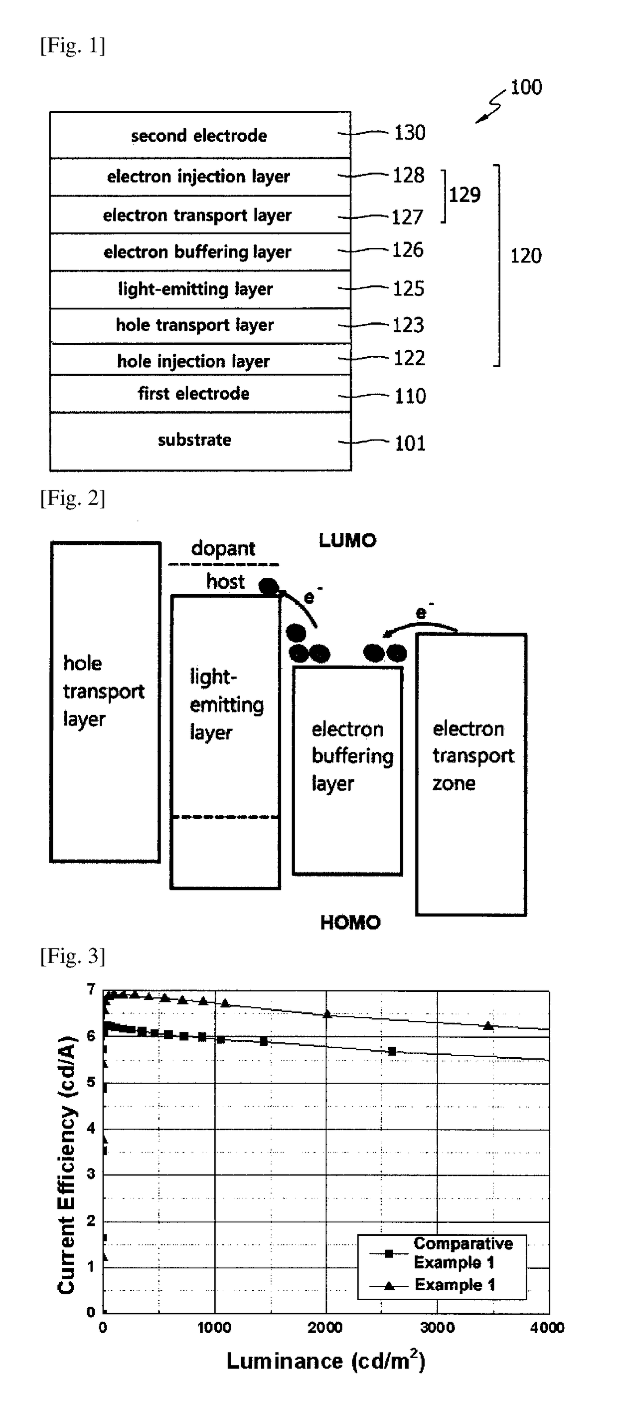
The present disclosure relates to an electron buffering material, and an organic electroluminescent device comprising a first electrode, a second electrode facing the first electrode, a light-emitting layer between the first electrode and the second electrode, and an electron transport zone and an electron buffering layer between the light-emitting layer and the second electrode. The organic electroluminescent device comprising the electron buffering material of the present disclosure has low driving voltage, excellent luminous efficiency, and long lifespan.
Description
TECHNICAL FIELD[0001]The present disclosure relates to an electron buffering material, an electron transport material and an organic electroluminescent device comprising the same.BACKGROUND ART[0002]An organic electroluminescent device (OLED) emitting green light was first proposed by Tang et al. of Eastman Kodak in 1987, which employs a double layer of TPD / Alq3, composed of a light-emitting layer and a charge transport layer. Afterward, an organic electroluminescent device had been rapidly researched, and has now become commercialized. At present, a phosphorescent material, which has excellent luminous efficiency, is mainly used for a panel of an organic electroluminescent device. An organic electroluminescent device emitting red or green light has been successfully commercialized by using a phosphorous material. However, a phosphorous material for emitting blue light has the following disadvantages, which are blocking realization of full color display: roll-off is reduced at high ...
Claims
Application Information
Patent Timeline
Application Date:The date an application was filed.
Publication Date:The date a patent or application was officially published.
First Publication Date:The earliest publication date of a patent with the same application number.
Issue Date:Publication date of the patent grant document.
PCT Entry Date:The Entry date of PCT National Phase.
Estimated Expiry Date:The statutory expiry date of a patent right according to the Patent Law, and it is the longest term of protection that the patent right can achieve without the termination of the patent right due to other reasons(Term extension factor has been taken into account ).
Invalid Date:Actual expiry date is based on effective date or publication date of legal transaction data of invalid patent.

