

Organic light emitting device
- Summary
- Abstract
- Description
- Claims
- Application Information
AI Technical Summary
Benefits of technology
Problems solved by technology
Method used
Image

Examples
example 1
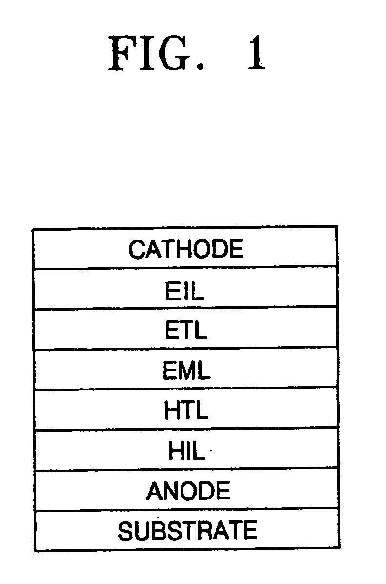
[0037] First, a Corning glass substrate at 15 Ω / cm2 coated with 1200 Å ITO anode material was cut to a size 50 mm×50 mm×0.7 mm. The resultant glass substrate was cleaned using ultrasonic waves in isopropyl alcohol for 5 minutes, cleaned using ultrasonic waves in pure water for 5 minutes, and cleaned using UV and ozone for 30 minutes. N,N′-di(1-naphtyl)-N,N′-diphenylbenxidine(NPD) was vacuum-evaporated on the substrate to form a hole transport layer to a thickness of about 600 Å.
[0038] 22 parts by weight of 2,5-dispirobifluorene-1,3,4-oxadiazole, 66 parts by weight of BAlq3, and 12 parts by weight of fr(pq)2(acac) were co-deposited on the hole transport layer to form an emission layer to a thickness of about 400 Å. Alq3 as an electron transport material was deposited on the emission layer to form an electron transport layer toga thickness of about 300 Å.
[0039] LiF was vacuum-evaporated on the electron transport layer to form an electron injection layer to a thickness of about 10 Å ...
example 2
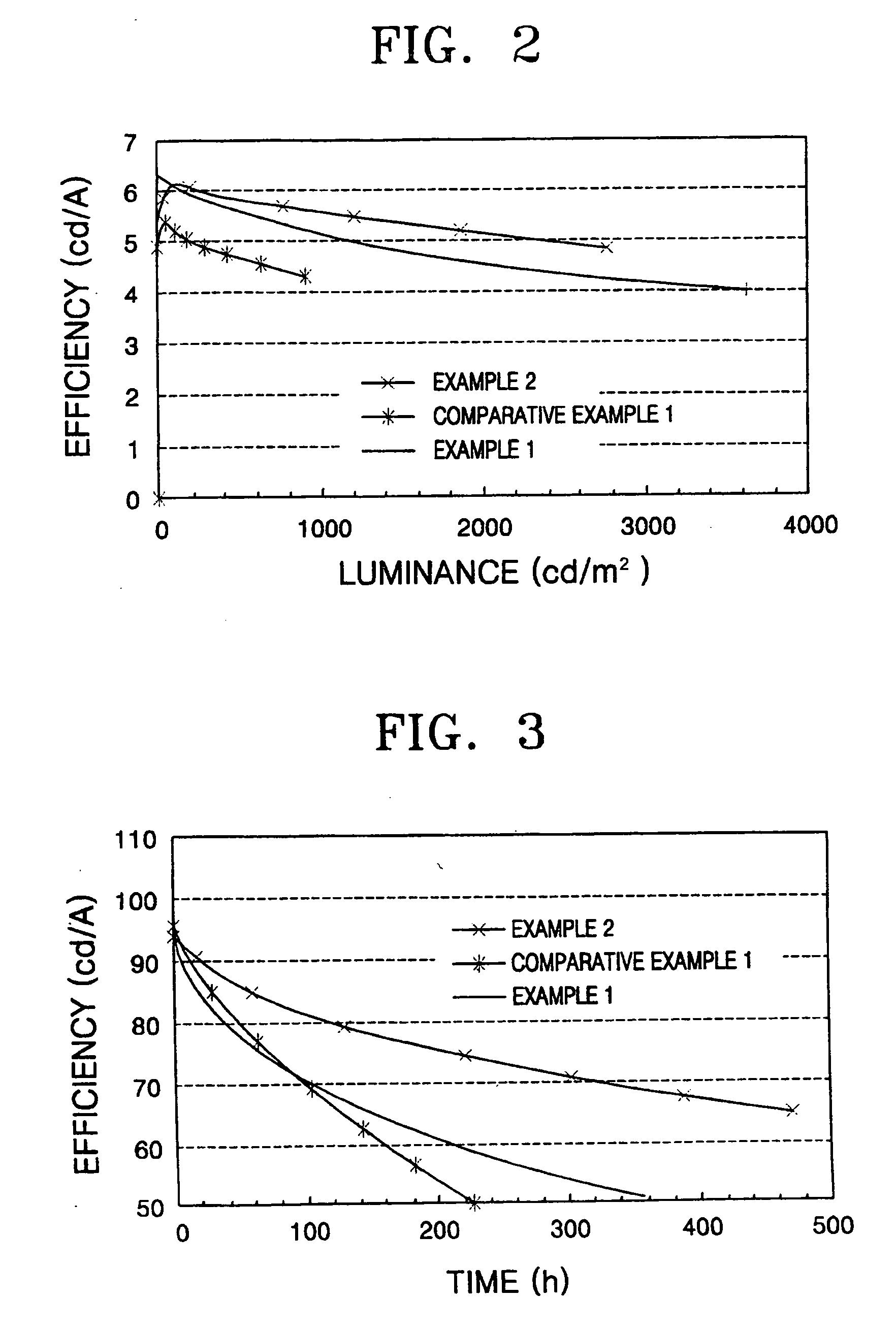
[0040] An organic light emitting device was manufactured in the same manner as in Example 1, except 66 parts by weight of 2,5-dispirobifluorene-1,3,4-oxadiazole and 22 parts by weight of BAlq3 were used.
PUM
| Property | Measurement | Unit |
|---|---|---|
| Percent by mass | aaaaa | aaaaa |
| Percent by mass | aaaaa | aaaaa |
| Percent by mass | aaaaa | aaaaa |
Abstract
Description
Claims
Application Information