Display device

a display device and active matrix technology, applied in the direction of instruments, static indicating devices, etc., can solve the problems of not being able to optimize the black luminance and the white luminance simultaneously, and achieve the effect of optimizing the black luminance and the white luminan

Inactive Publication Date: 2007-08-16
JAPAN DISPLAY WEST
View PDF14 Cites 43 Cited by
  • Summary
  • Abstract
  • Description
  • Claims
  • Application Information

AI Technical Summary

Benefits of technology

[0040] According to the present invention, there is the advantage to being

Problems solved by technology

Due to this, in current liquid crystal display devices employing the capacity coupling drive system, there

Method used


Image

  • Display device
  • Display device
  • Display device

Examples


Embodiment Construction

[0074] Below, embodiments of the present invention will be explained with reference to the figures.

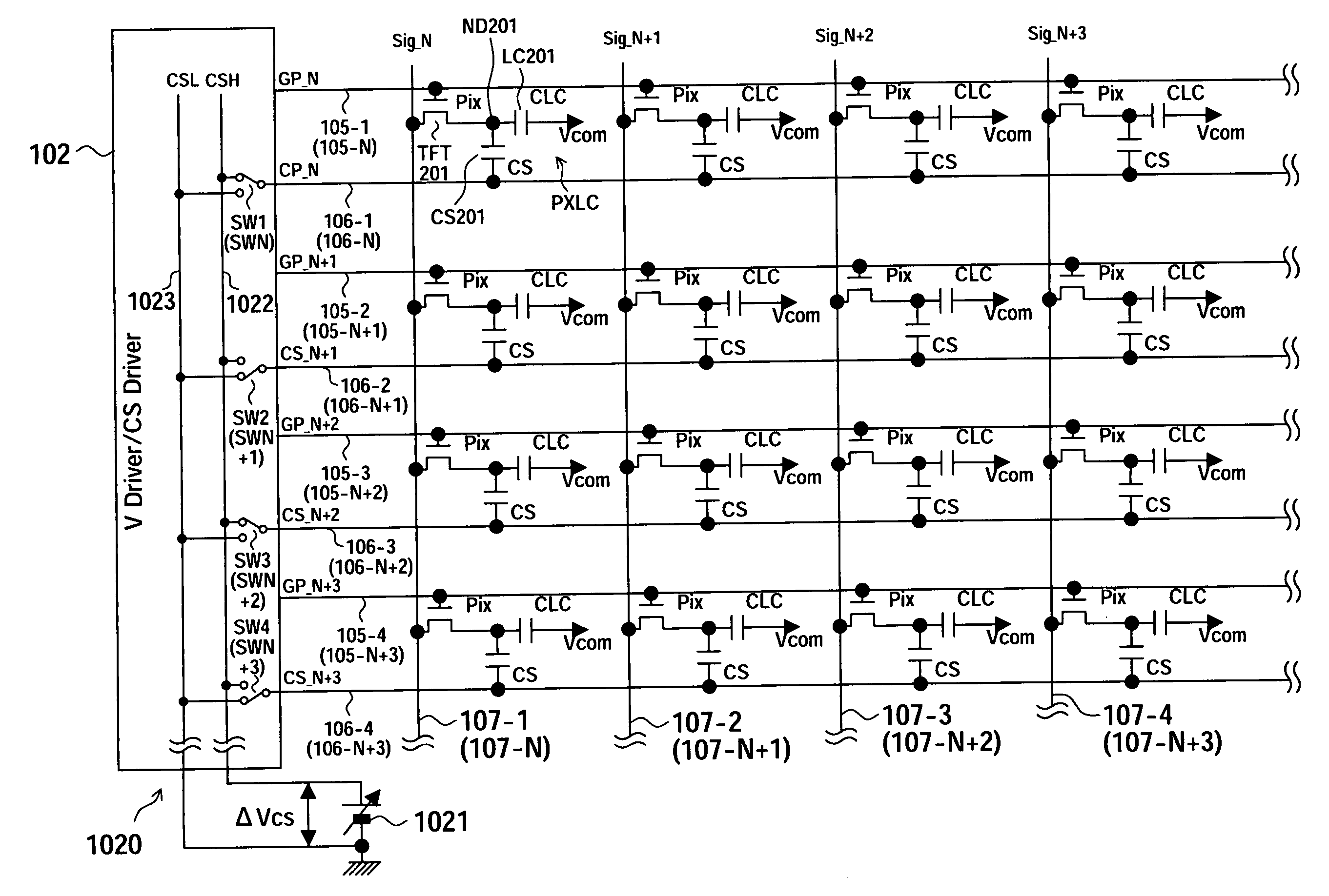
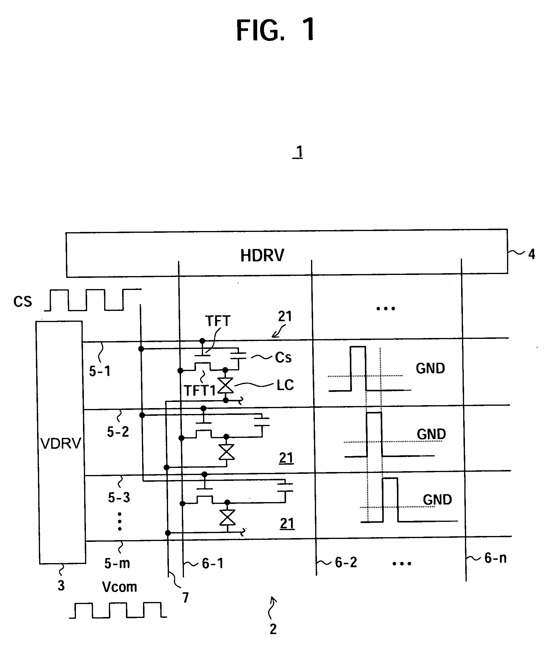
[0075]FIG. 6 is a view showing an example of the configuration of an active matrix type display device according to a first embodiment of the present invention using for example liquid crystal cells as display elements of pixels (electrooptic elements).

[0076] The display device 100, as shown in FIG. 6 to FIG. 8, has as its main constituent elements an effective pixel section 101, a vertical drive circuit (VDRV) 102, a horizontal drive circuit (HDRV) 103, a common voltage generation circuit (VcomGen) 104, gate lines (scan lines) 105-1 to 105-m, storage capacitor lines (hereinafter referred to as the “storage lines”) 106-1 to 106-m, signal lines 107-1 to 107-n, a dummy pixel section (monitor part) 108, and a detection circuit 109.

[0077] The effective pixel section 101, as shown in FIG. 7 and FIG. 8, has a plurality of pixel circuits PXLC arrayed in an m×n matrix. Specifically, to enab...


PUM


Abstract

A display device having a pixel section pixel circuits, scan lines, capacity lines, a drive circuit driving the scan lines and the capacity lines selectively, a generation circuit generating a common voltage signal switching in level at a predetermined cycle, and a correction circuit correcting the signals driving the capacity lines of the drive circuit, wherein each pixel circuit contains a display element and holding capacitor, a first pixel electrode of the display element pixel cell, a first electrode of the holding capacitor, and one terminal of the switching element are connected, a second electrode of the holding capacitor is connected to the capacity lines arrayed in a corresponding row, and the common voltage signal is applied in a second pixel electrode of the display element. The correction circuit has a monitor circuit monitoring the pixel potential of the pixel section and correcting a signal driving the capacity lines taking into consideration the optical characteristics of the display element based on the monitor result of the monitor circuit.

Description

CROSS REFERENCE TO RELATED APPLICATION [0001] The present invention contains subject matter related to Japanese Patent Applications No. 2005-228739, No. 2005-228740 filed in the Japan Patent Office on Aug. 5, 2005, and No. 2005-234826 filed in the Japan Patent Office on Aug. 12, 2005, the entire contents of which being incorporated herein by reference. BACKGROUND OF THE INVENTION [0002] 1. Field of Invention [0003] The present invention relates to an active matrix-type display device having display elements of pixels (electrooptic elements) arrayed in a display region in a matrix. [0004] 2. Description of the Related Art [0005] Display devices, for example, liquid crystal display devices using liquid crystal cells for the display elements of the pixels (electrooptic elements), feature thin profiles and low power consumptions. Utilizing these features, they are being used in, for example, personal digital assistants (PDAs), mobile phones, digital cameras, video cameras, personal comp...

Claims


Application Information

Patent Timeline
IPC IPC(8): G09G3/36
CPCG09G3/3677G09G3/3688G09G2320/0252G09G2310/0278G09G2320/0223G09G3/3696
Inventor SATO, TOMOHIKOITAKURA, NAOYUKITAKEUCHI, TAKEYAFUKANO, TOMOYUKI
Owner JAPAN DISPLAY WEST
Why Eureka
Try Eureka