Display device

a display device and display technology, applied in the field of display devices, to achieve the effect of simple circuit configuration

Active Publication Date: 2007-08-16
PANASONIC LIQUID CRYSTAL DISPLAY CO LTD +1
View PDF5 Cites 3 Cited by
  • Summary
  • Abstract
  • Description
  • Claims
  • Application Information

AI Technical Summary

Benefits of technology

[0026]According to the present invention, it is possible to provide a display device that is equipped with a dr

Problems solved by technology

2002-287711 suffers from such a problem that a space is broadened because the number of transistor elements is large, and therefore the l

Method used


Image

  • Display device
  • Display device
  • Display device

Examples


Embodiment Construction

[0039]Now, a description will be given in more detail of preferred embodiments of the present invention with reference to the accompanying drawings.

[0040]In all of drawings for explaining the embodiment, parts having the same functions are denoted by identical symbols, and their duplicated description will be omitted.

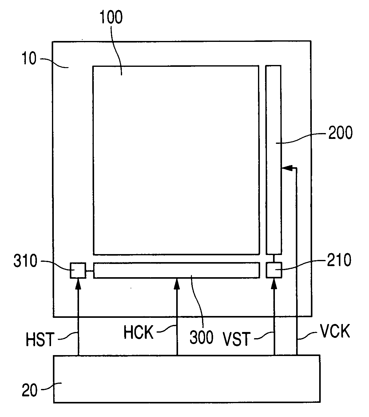
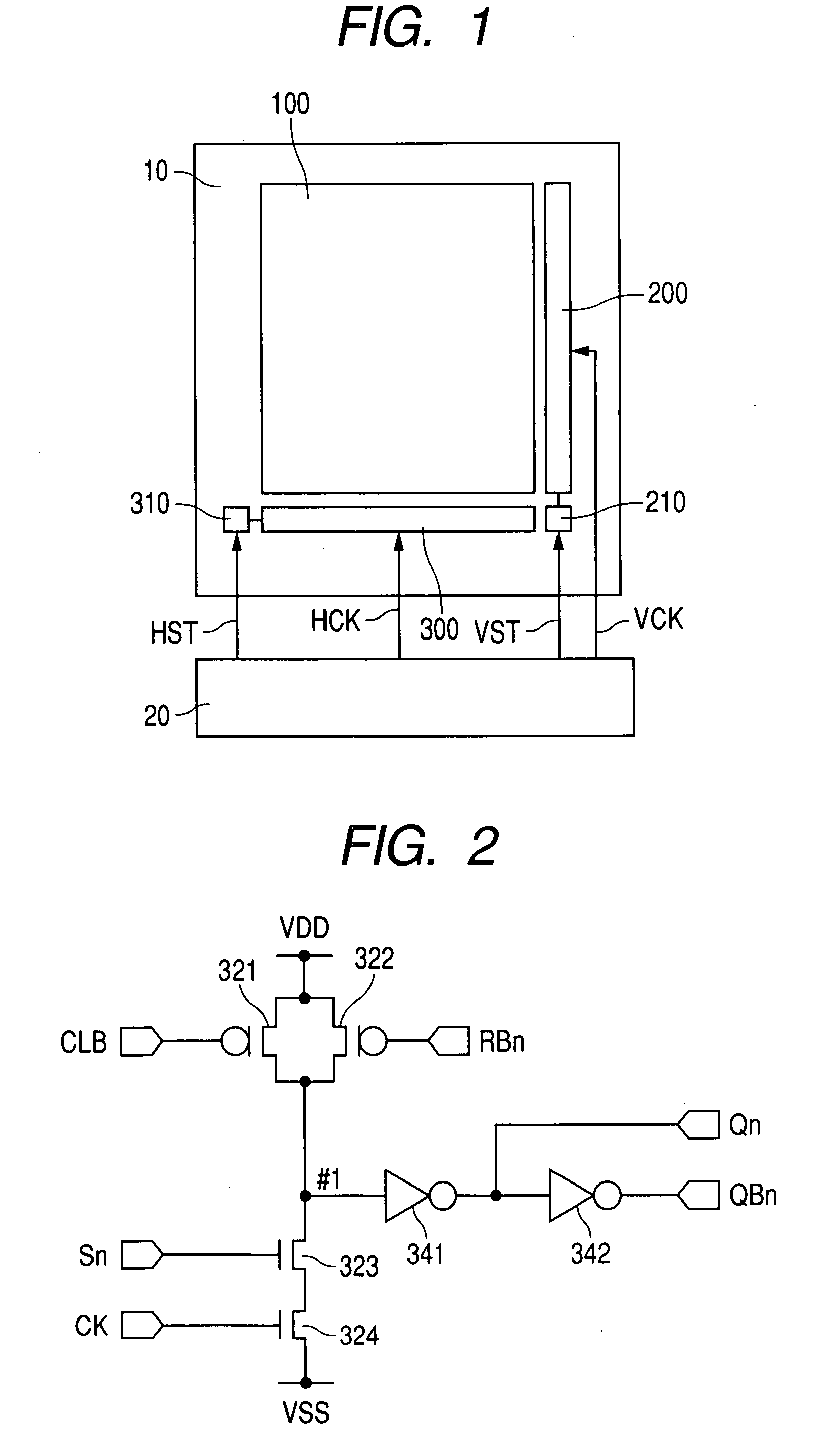
[0041]FIG. 1 is a block diagram showing the outline configuration of a liquid crystal display module according to an embodiment of the present invention.

[0042]In the drawing, reference numeral 10 denotes a liquid crystal display panel, and 20 is a control circuit. The liquid crystal display panel 10 includes a display section 100, a gate circuit 200, a level converter circuit 210 of the gate circuit 200, a drain circuit 300, and a drain converter circuit 310 of the drain circuit 300.

[0043]The control circuit 20 outputs a start signal (VST) of the gate circuit 200, a clock signal (VCK), a start signal (HST) of the drain circuit, and a clock signal (HCK). In this example,...


PUM


Abstract

A shift register circuit having a level conversion function is provided with a simple circuit configuration. Each basic circuit of the shift register circuit includes: a first transistor of a second conductivity type having a first electrode to which a second supply voltage is applied; a second transistor of the second conductivity type having a first electrode connected to a second electrode of the first transistor and a second electrode connected to an output node; a third transistor of a first conductivity type having a first electrode to which a first supply voltage is applied and a second electrode connected to the output node directly or through another transistor, the first conductivity type being different from the second conductivity type; and a fourth transistor of the first conductivity type having a first electrode to which the first supply voltage is applied and a second electrode connected to the second electrode of the third transistor, wherein a clock signal is supplied to a control electrode of the first transistor, a set signal is supplied to a control electrode of the second transistor, a clear signal is supplied to a control electrode of the third transistor, a reset signal is supplied to a control electrode of the fourth transistor, and a voltage of the output node is an output of a scanning circuit.

Description

CLAIM OF PRIORITY[0001]The present application claims priority from Japanese Application JP 2006-037604 filed on Feb. 15, 2006, the content of which is hereby incorporated by reference into this application.BACKGROUND OF THE INVENTION[0002]1. Field of the Invention[0003]The present invention relates to display devices, and more particularly to a display device that is equipped with a driver circuit having a shift register circuit with a level conversion function.[0004]2. Description of the Related Art[0005]In general, in an active matrix liquid crystal display device using a thin film transistor (TFT: thin film transistor) as an active element, a scanning circuit is used to sequentially apply a selected scanning voltage to scanning lines.[0006]Up to now, as a shift register circuit that is used in the above scanning circuit, there has been known a shift register circuit having a level converter circuit of the differential circuit system, for example, as disclosed in Japanese Patent ...

Claims


Application Information

Patent Timeline
IPC IPC(8): G02F1/1333
CPCG09G3/3677G09G2310/0289G09G3/3688
Inventor SATO, HIDEONISHITANI, SHIGEYUKINAKAO, TAKAYUKIMAKI, MASAHIRO
Owner PANASONIC LIQUID CRYSTAL DISPLAY CO LTD
Why Eureka
Try Eureka