Method for etching silicon-germanium in the presence of silicon

US20070190787A1Active Publication Date: 2007-08-16STMICROELECTRONICS SRL

Image

  • Method for etching silicon-germanium in the presence of silicon
  • Method for etching silicon-germanium in the presence of silicon

Examples


Embodiment Construction

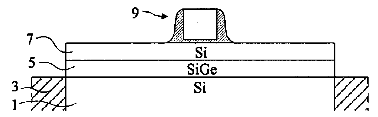
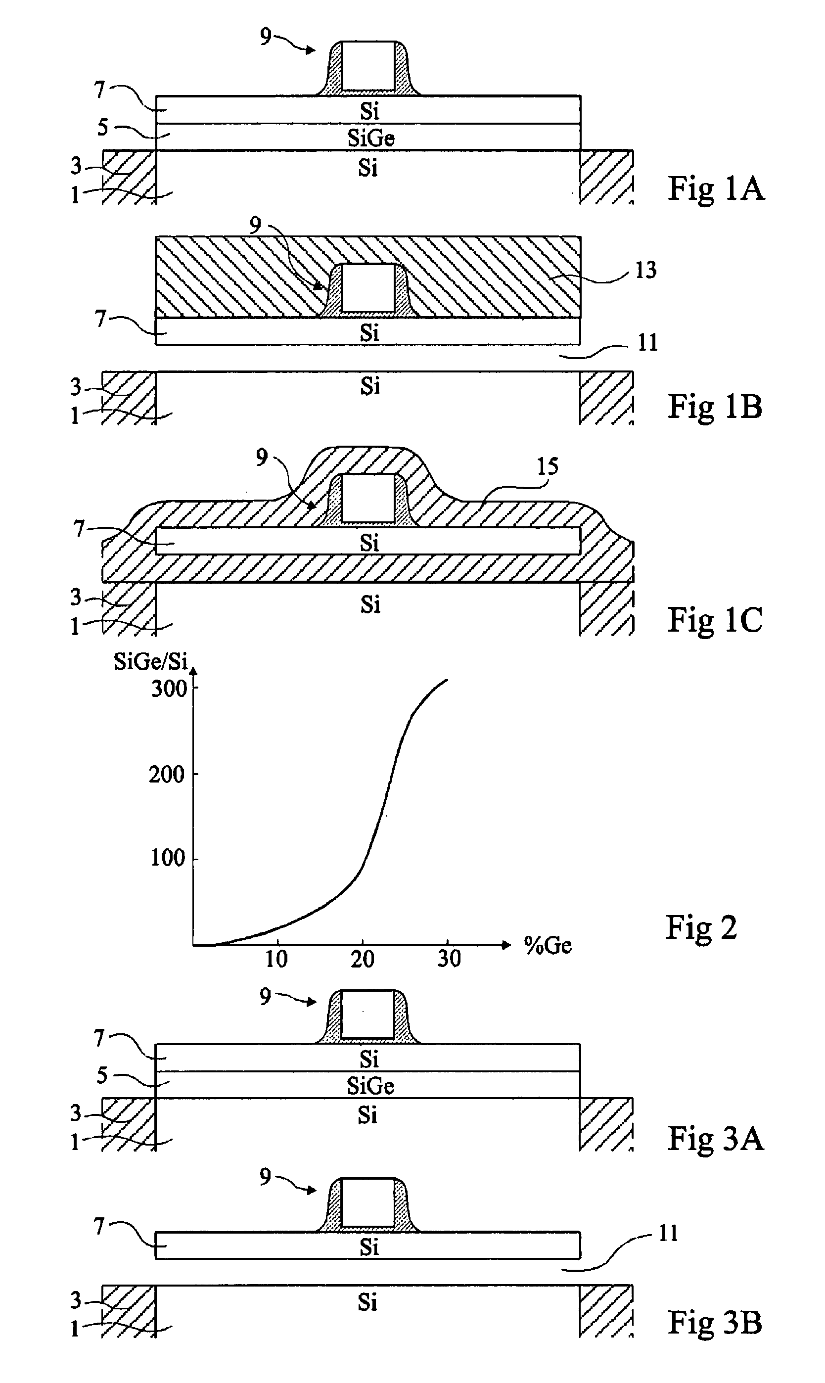
[0036]As usual in the representation of semiconductor components, the various cross-section views are not to scale.

[0037]The present invention provides a method that is very selective for etching silicon-germanium with respect to silicon.

[0038]The present invention provides, in a method of chemical vapor etch type (CVE) using hydrochloric acid as an etchant.

[0039]This type of method is typically used to etch silicon and it was thus not envisaged to use it to etch a material (silicon-germanium) selectively with respect to silicon. However, against this prejudice, the applicant has performed comparative tests of silicon and silicon-germanium CVE etching with hydrochloric acid.

[0040]The applicant has noted that, in very wide usual pressure ranges, the etch speed of silicon drops below 0.10 nm / minute when the processing temperature falls below 700° C. This speed increases exponentially when the temperature increases above 700° C. Still in a wide pressure range, the etch speed of silicon...


PUM


Abstract

A method for selectively etching single-crystal silicon-germanium in the presence of single-crystal silicon, including a chemical etch based on hydrochloric acid in gaseous phase at a temperature lower than approximately 700° C.

Description

BACKGROUND OF THE INVENTION[0001]1. Field of the Invention[0002]The present invention relates to the manufacturing of semiconductor circuits. More specifically, the present invention relates to the selective etching of single-crystal silicon-germanium (SiGe) in the presence of single-crystal silicon.[0003]2. Discussion of the Related Art[0004]One often has to etch a single-crystal silicon-germanium layer in the presence of single-crystal silicon.[0005]For example, it has been provided to use silicon-germanium as a sacrificial layer interposed between a single-crystal semiconductor substrate and a single-crystal silicon layer to obtain a floating single-crystal silicon layer of very low thickness, for example, lower than 20 nm. This floating silicon layer is currently designated as an SON layer (for Silicon On Nothing).[0006]Such an SON substrate can be used on forming of various components such as, for example, MOS transistors and microresonators.[0007]For a better understanding of ...

Claims


Application Information

Patent Timeline
16 Aug 2007
Publication
US20070190787A1
IPC
H01L21/302
CPC
H01L21/3065; H01L21/306
Inventors
LOUBET, NICHOLAS; DUTARTRE, DIDIER