Semiconductor memory device and method of manufacturing the same
a memory device and semiconductor technology, applied in the direction of semiconductor devices, electrical devices, transistors, etc., can solve the problems of decrease of electric capacitance, and faulty operation of memory devices
- Summary
- Abstract
- Description
- Claims
- Application Information
AI Technical Summary
Problems solved by technology
Method used
Image

Examples
first embodiment
[0028] In a first embodiment, a radical nitride film is formed by radical nitriding on an interelectrode insulating film between a floating gate electrode and control gate electrode.
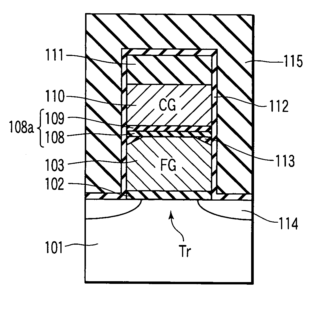
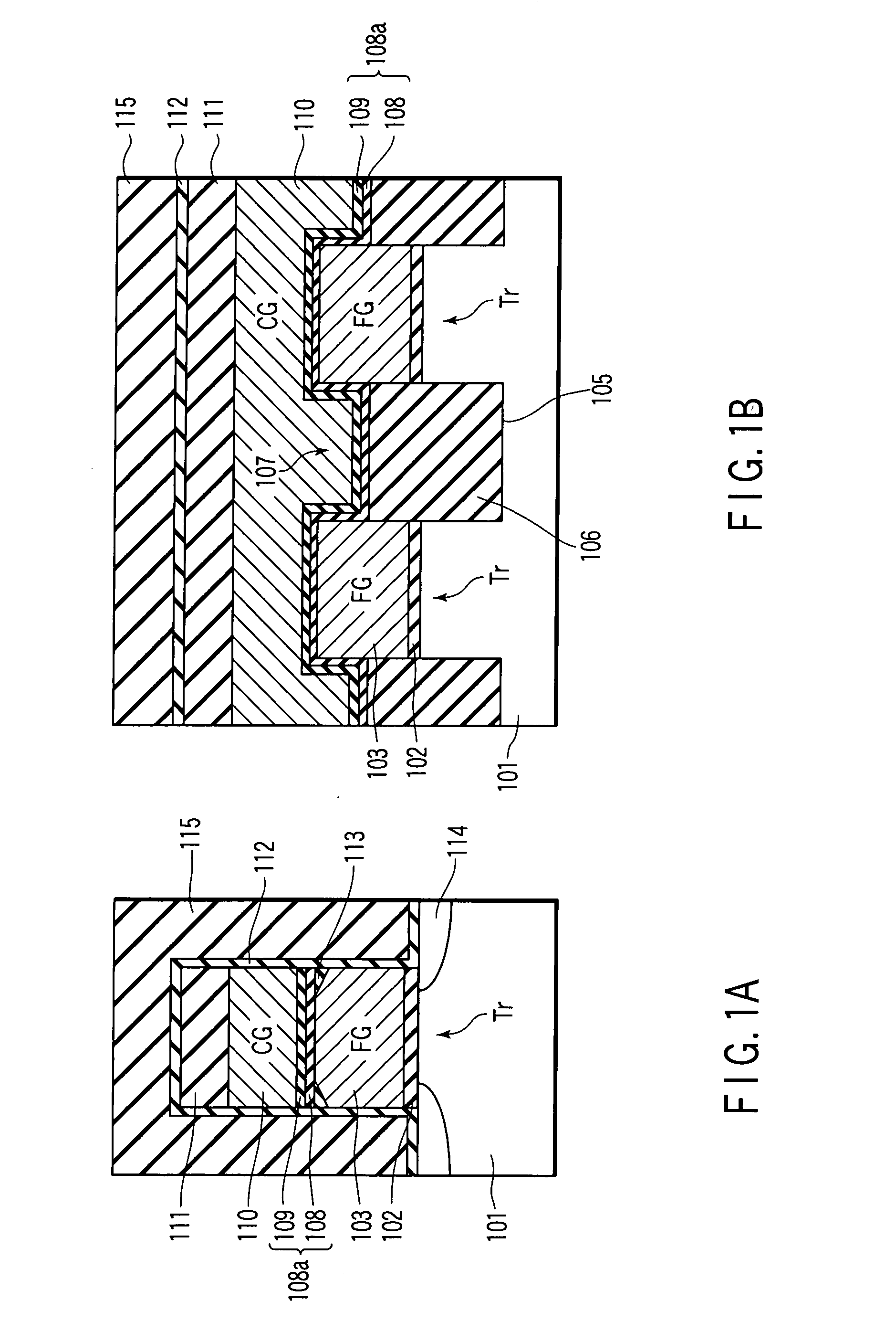
[0029]FIGS. 1A and 1B are sectional views of a nonvolatile semiconductor memory device according to the first embodiment of the present invention. FIG. 1A is a sectional view in the bit line direction (channel length direction), and FIG. 1B is a sectional view in the word line direction (channel width direction). This nonvolatile semiconductor memory device according to the first embodiment will be explained below.
[0030] As shown in FIGS. 1A and 1B, floating gate electrodes FG are formed on a silicon substrate 101 via a tunnel oxide film 102, and an interelectrode insulating film 108 is formed on the floating gate electrodes FG. A radical nitride film 109 is formed on the interelectrode insulating film 108 by radical nitriding. A control gate electrode CG is formed on the radical nitride film 109, and ...
second embodiment
[0050] In the first embodiment, the radical nitride film is formed only on the interelectrode insulating film. In a second embodiment, however, radical nitride films are formed above and below an interelectrode insulating film.
[0051]FIGS. 8A and 8B are sectional views of a nonvolatile semiconductor memory device according to the second embodiment of the present invention. FIG. 8A is a sectional view in the bit line direction (channel length direction), and FIG. 8B is a sectional view in the word line direction (channel width direction). This nonvolatile semiconductor memory device according to the second embodiment will be explained below.
[0052] As shown in FIGS. 8A and 8B, the second embodiment differs from the first embodiment in that a radical nitride film 109 is formed above an interelectrode insulating film 108, and a radical nitride film 120 is formed below the interelectrode insulating film 108. When oxidation is performed to form a gate sidewall oxide film 112, therefore, ...
third embodiment
[0069] If a structure (to be referred to as an NONON structure hereinafter) having radical nitride films 109 and 120 above and below an interelectrode insulating film 108 made of an ONO film is formed when a trench 107 between adjacent floating gates FG1 and FG2 has a high aspect ratio and a narrow opening, a film thickness Tside of the radical nitride film 120 (120a) on the sidewall surfaces of the trench 107 sometimes decreases in a portion X (a side-surface portion in the lower portion of the trench 107) in the lower portion of the floating gate electrode FG1 (FG2) (FIG. 13). This is presumably because radical nitriding hardly reaches the bottom of the trench 107 to make the supply amount of radical nitriding insufficient. If this is the case, an electric charge leak between the floating gate electrode FG and a control gate electrode CG in the portion X may increase to worsen the charge retention characteristics.
[0070] To solve the above problem, a third embodiment uses means (1...
PUM
 Abstract
Description
Claims
Application Information
 - R&D Engineer
- R&D Manager
- IP Professional
- Industry Leading Data Capabilities
- Powerful AI technology
- Patent DNA Extraction
Browse by: Latest US Patents, China's latest patents, Technical Efficacy Thesaurus, Application Domain, Technology Topic.
© 2024 PatSnap. All rights reserved.Legal|Privacy policy|Modern Slavery Act Transparency Statement|Sitemap