

Method for cleaning reaction chamber using pre-cleaning process
a reaction chamber and pre-cleaning technology, applied in the direction of cleaning hollow articles, chemistry apparatus and processes, coatings, etc., can solve the problems of halide cleaning gas not being effective, deteriorating the quality of the film on the substrate, and damage to the electrodes, so as to increase the efficiency of the cleaning step
- Summary
- Abstract
- Description
- Claims
- Application Information
AI Technical Summary
Benefits of technology
Problems solved by technology
Method used
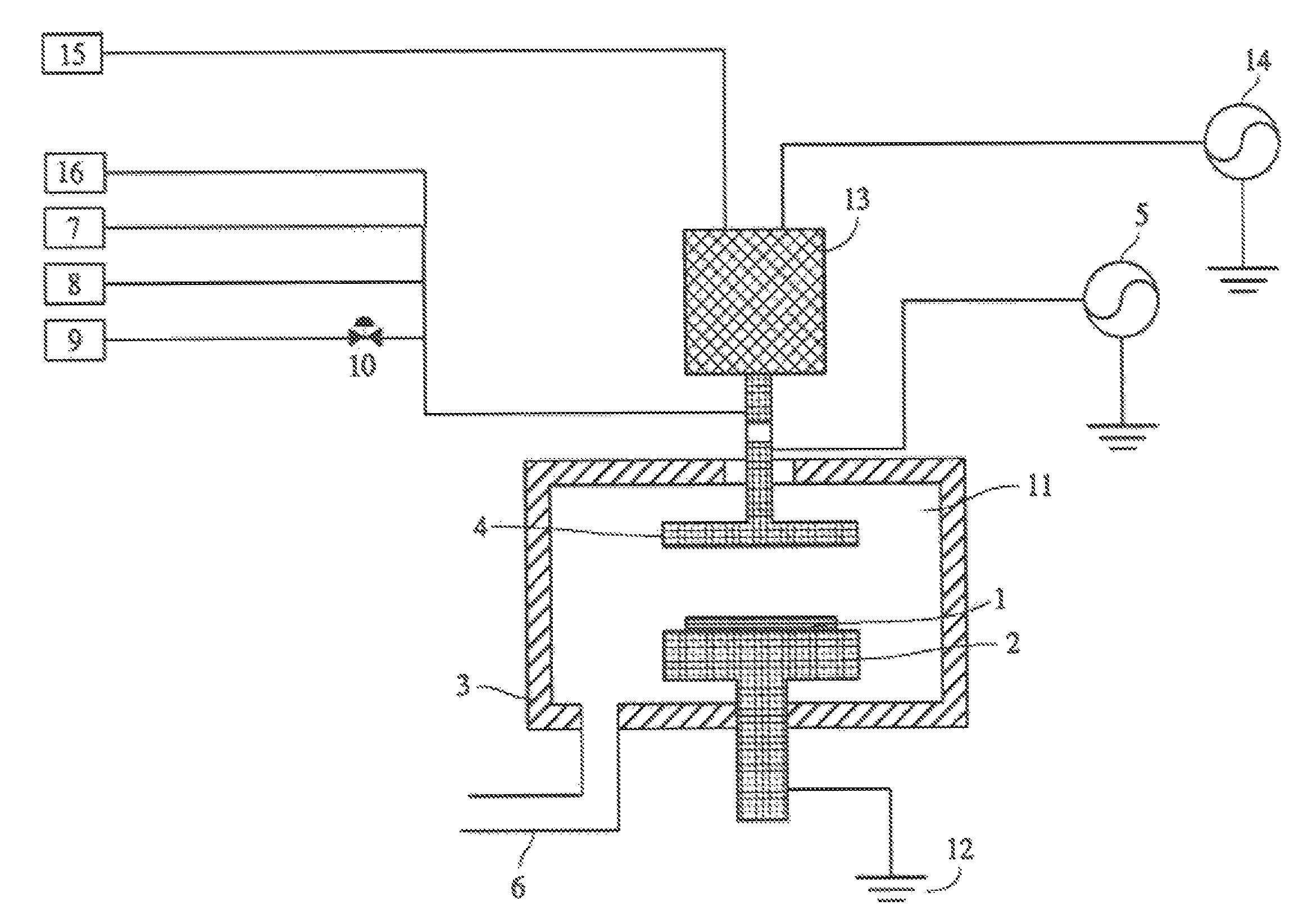
Image

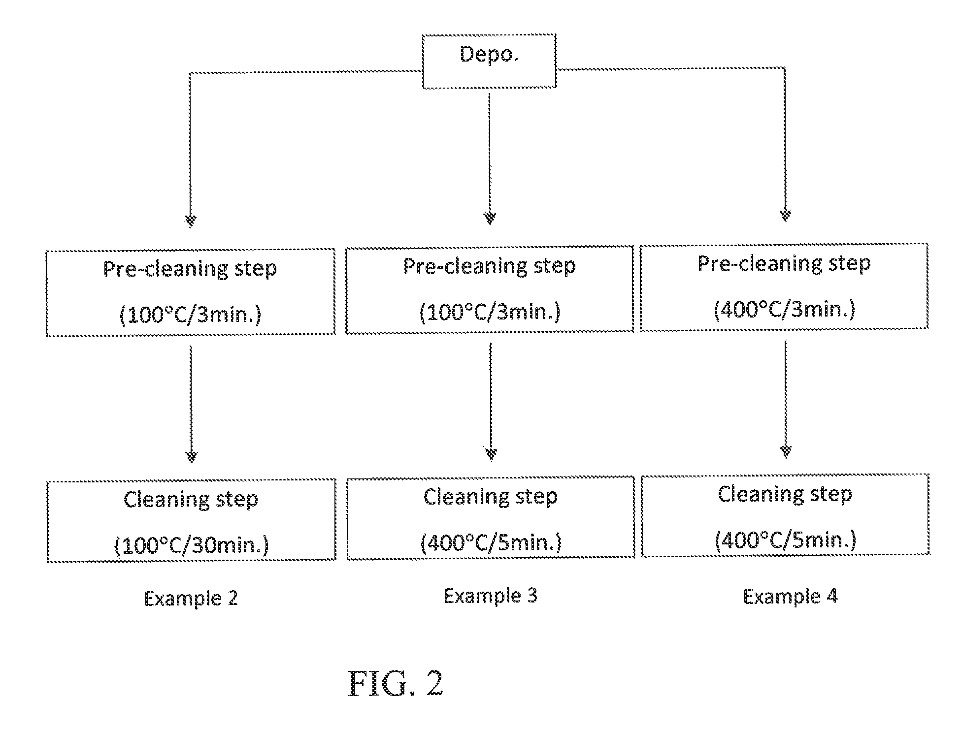
Examples
example 1
Comparative Example
[0051]No pre-cleaning step was conducted. After the deposition, a cleaning step began under the conditions shown in FIG. 4 below.
[0052]
TABLE 4CleaningPressure [Pa]1000Tem. [° C.]100Preprocess gasNF3Gas flow [sccm]1000Other gasArGas flow [sccm]4000RF power [W]Remote PlasmaDuration [min]30
example 2
[0053]A pre-cleaning step was conducted under the conditions shown in Table 5 below, and then, a cleaning step was conducted under the same conditions as those shown in Table 4.
[0054]
TABLE 5Pre-cleaning stepPressure [Pa]200Tem. [° C.]100Pre-cleaning gasO2Gas flow [sccm]l000Other gasArGas flow [sccm]1000RF power [W]200RF frequency13.56 MHzDuration [min]3
example 3
[0055]A pre-cleaning step was conducted under the same conditions as those shown in Table 5, and then, a cleaning step was conducted under the conditions shown in Table 6 below.
[0056]
TABLE 6CleaningPressure [Pa]1000Tem. [° C.]400Preprocess gasNF3Gas flow [sccm]1000Other gasArGas flow [sccm]1000RF power [W]Remote PlasmaDuration [min]5
PUM
| Property | Measurement | Unit |
|---|---|---|
| temperature | aaaaa | aaaaa |
| thickness | aaaaa | aaaaa |
| thickness | aaaaa | aaaaa |
Abstract
Description
Claims
Application Information