

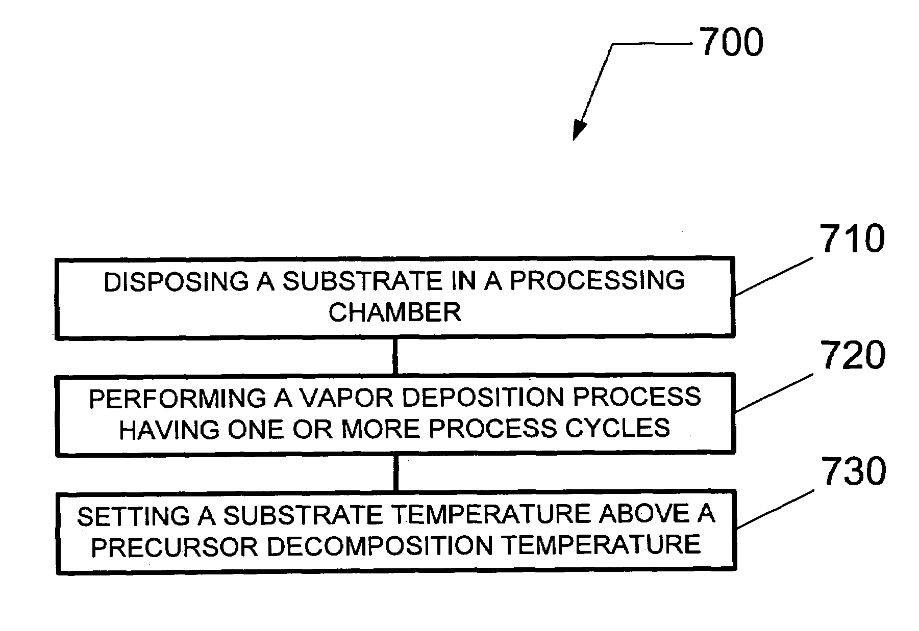
Method of forming a metal carbide or metal carbonitride film having improved adhesion
a metal carbide or metal carbonitride film technology, applied in the field of thin film formation, can solve the problems of poor adhesion, poor barrier properties, time-consuming current ald processes, etc., and achieve the effect of improving adhesion properties and facilitating the vapor deposition process
- Summary
- Abstract
- Description
- Claims
- Application Information
AI Technical Summary
Benefits of technology
Problems solved by technology
Method used
Image

Examples
Embodiment Construction
[0019]In the following description, in order to facilitate a thorough understanding of the invention and for purposes of explanation and not limitation, specific details are set forth, such as a particular geometry of the deposition system and descriptions of various components. However, it should be understood that the invention may be practiced in other embodiments that depart from these specific details.
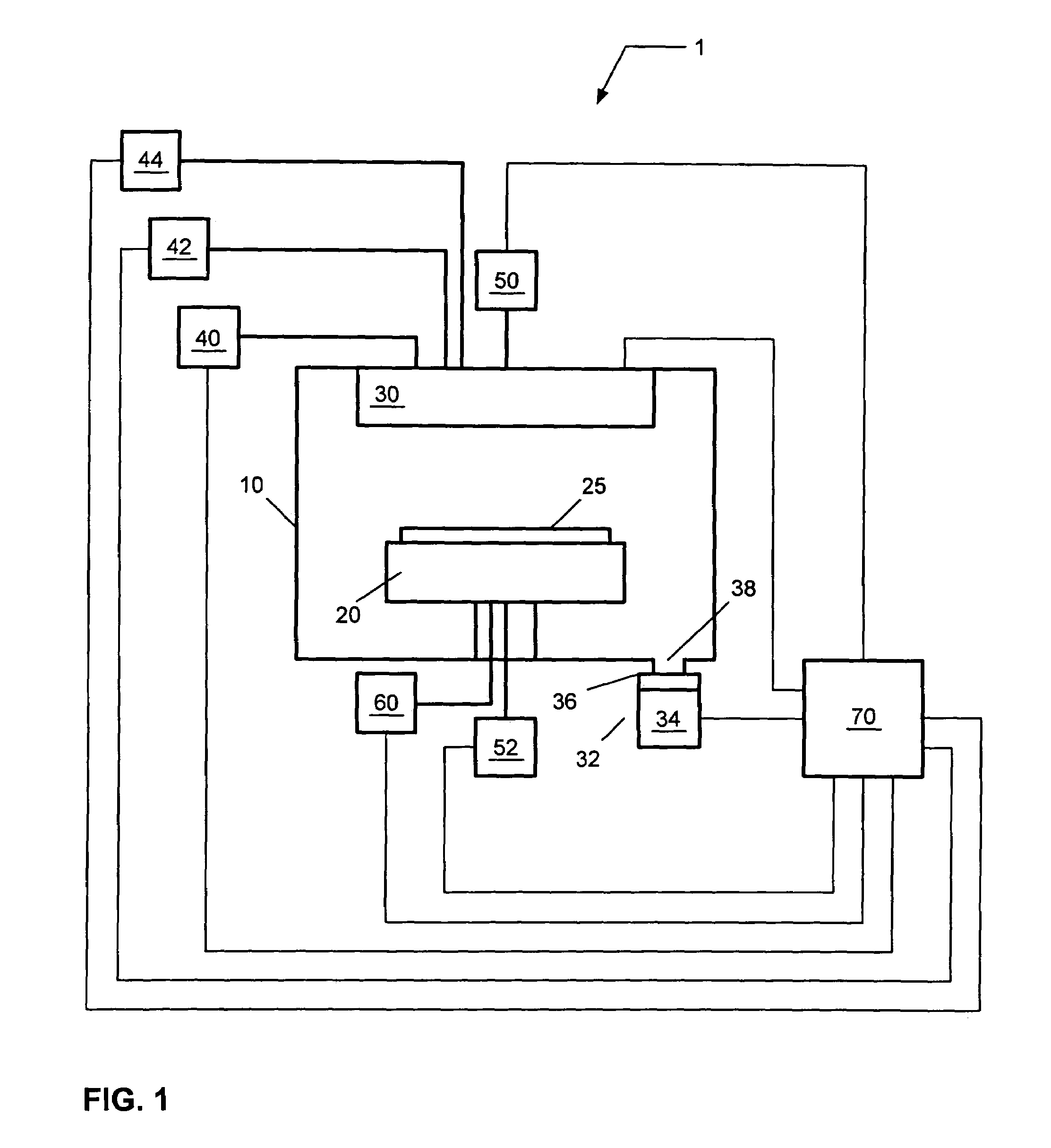
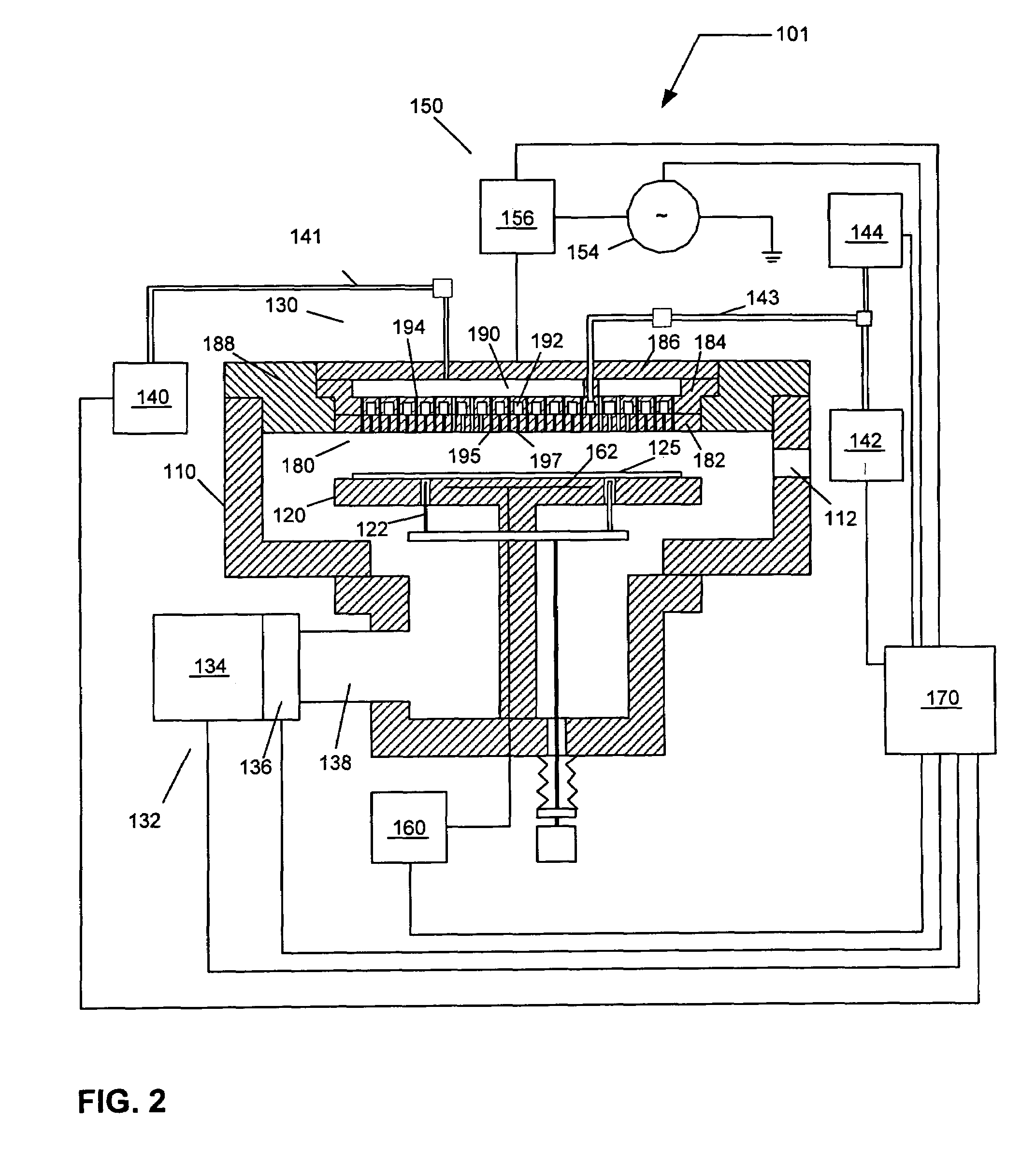
[0020]Referring now to the drawings, wherein like reference numerals designate identical or corresponding parts throughout the several views, FIG. 1 illustrates a deposition system 1 for depositing a thin film on a substrate according to one embodiment. For example, during the metallization of inter-connect and intra-connect structures for semiconductor devices in back-end-of-line (BEOL) operations, a thin conformal barrier layer may be deposited on wiring trenches or vias to minimize the migration of metal into the inter-level or intra-level dielectric.
[0021]The deposition system...
PUM
| Property | Measurement | Unit |
|---|---|---|
| frequencies | aaaaa | aaaaa |
| RF frequency | aaaaa | aaaaa |
| RF frequency | aaaaa | aaaaa |
Abstract
Description
Claims
Application Information