Workpiece size measurement method and apparatus

a workpiece size and measurement method technology, applied in material analysis using wave/particle radiation, instruments, nuclear engineering, etc., can solve problems such as insatisfactory measurement of currently existing complex multi-layered circuit elements, prior technique approaches fail to take into account, and applicability suffers

Active Publication Date: 2007-09-27
HITACHI HIGH-TECH CORP
View PDF4 Cites 75 Cited by
  • Summary
  • Abstract
  • Description
  • Claims
  • Application Information

AI Technical Summary

Benefits of technology

[0006] One major object of the present invention is to provide a workpiece size measuring method and apparatus suitably adapted for length measurement of multilayered circuit elements with increased complexities.
[0007] According to this invention, in order to attain the foregoing object, methodology and apparatus are proposed for changing measurement conditions in a way pursuant to a workpiece image or the situation of a semiconductor circuit element to be measured when measuring pattern sizes on a workpiece image by use of design data of the semiconductor circuit element. With such an arrangement, appropriate measurement conditions are selectable in accordance with the state of workpiece image and / or the state of a circuit element formed on the workpiece, thereby making it possible to improve the measurement efficiency.

Problems solved by technology

Unfortunately, this approach suffers from problems which follow.
Unfortunately, the prior technique approach as taught by JP-A-2001-338304 (U.S. Pat. No. 6,868,175) is not satisfactory for performing measurement of the currently existing complicated multilayered circuit elements.
Another reason is that the prior technique approach fails to take into consideration the fact that a semiconductor circuit element is formed to span more than two stacked layers.

Method used


Image

  • Workpiece size measurement method and apparatus
  • Workpiece size measurement method and apparatus
  • Workpiece size measurement method and apparatus

Examples


embodiment 1

[0054] An example for measurement of the distance between an edge portion of scanning electron microscope (called SEM edge hereinafter) and design data will be explained with reference to some of the accompanying drawings below. This example will be referred to as Edge Placement Error (EPE) measurement in some cases.

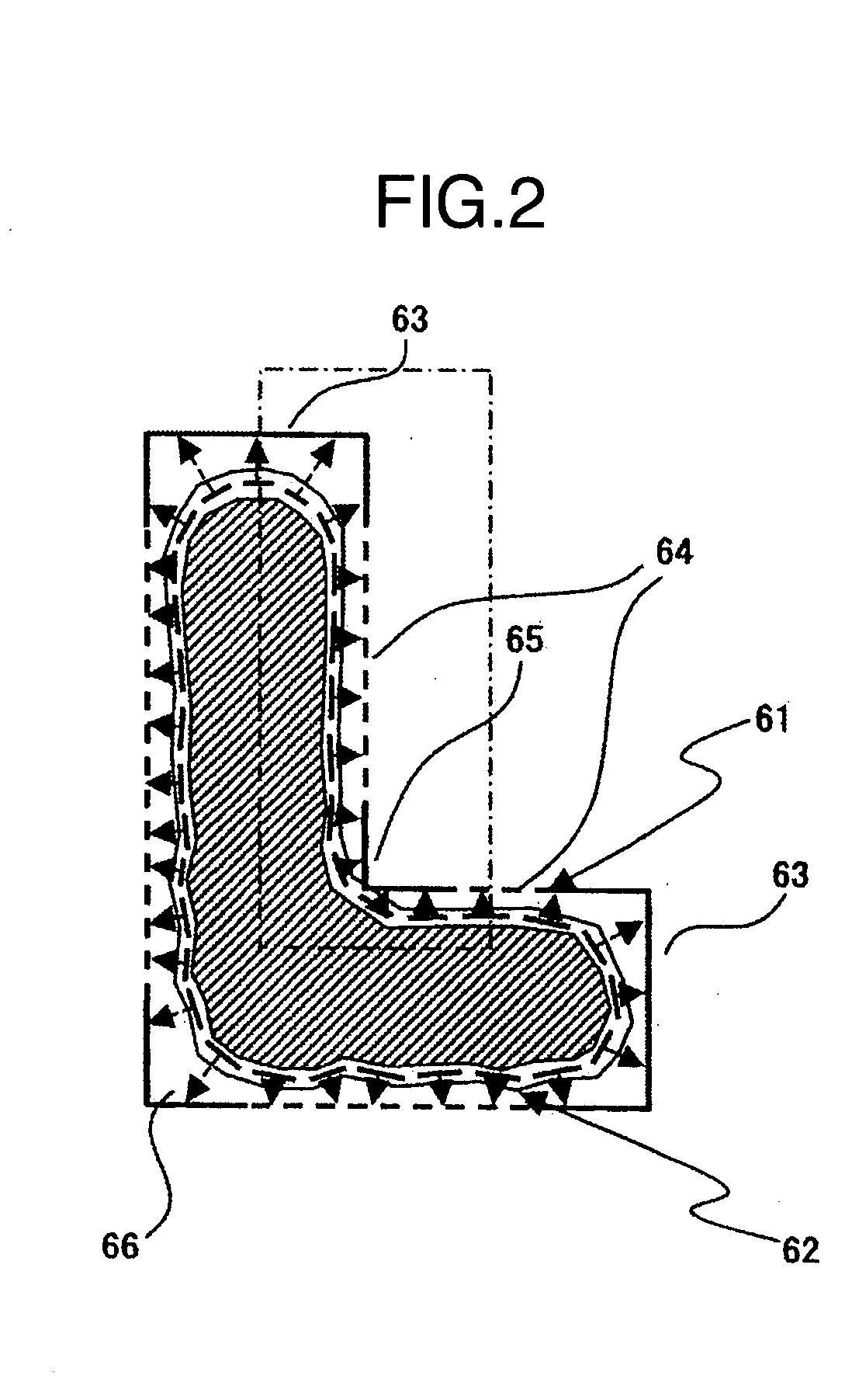
[0055]FIG. 2 is a diagram showing a state in which the design data and a SEM image are laid over each other. While EPE measurement is the one that measures the distance between design data and SEM edge, it is often the case that the real semiconductor circuit element is formed so that a rectangular corner of pattern is deformed and corrupted into a rounded shape, for example. Upon execution of EPE measurement for such corner-rounded pattern, it is sometimes difficult to judge the exact direction along which the measurement is to be done.

[0056] In this example, in view of such problem, it is proposed to determine the length measurement direction when performing EPE meas...

embodiment 2

[0088] An explanation will be given of an example which determines sampling points based on a length measurement result between design data and a Scanning Electron Microscope (SEM) edge, with reference to some of the accompanying drawings below. As shown in FIG. 2, when performing Edge Placement Error (EPE) measurement of a single pattern, a great number of candidates for the length measurement reference position are considered. However, the evaluation of a pattern from among all the measurement reference position candidates consumes much time and requires troublesome manual operations—this is not preferable in a viewpoint of measurement efficiency. On the other hand, it is very difficult to predetermine how a pattern will change from its ideal shape (design data): there is no guarantee that a measurement reference position as set up by a recipe is always the adequate length measurement location.

[0089] In this example, in view of the above-noted problem, it is proposed to perform l...

embodiment 3

[0093] An example which categorizes length measurement results based on the state of design data concerning length measurement positions thereof will be explained with reference to some of the drawings below. FIG. 8 shows an example with a plurality of patterns being formed into a multilayered structure and is a drawing showing a display example wherein design data 82, 83 of an under layer and target layer are laid over a SEM image of a pattern having a poly-gate (target layer) 81 that is multilayered above an active area (under layer) 80.

[0094] When performing EPE measurement for a composite pattern making up a semiconductor circuit element, a very large number of measurement reference position candidates exist. However, it is not preferable in the viewpoint of measurement efficiency to evaluate the pattern based on length measurement results of all such measurement reference position candidates consumes much time and labors.

[0095] Below is an explanation about an example which r...


PUM

PropertyMeasurementUnit
lengthaaaaaaaaaa
pattern lengthaaaaaaaaaa
statistical processingaaaaaaaaaa

Abstract

A workpiece size measurement method suitable for length measurement of multilayered circuit elements with increased complexities is disclosed. This method employs a technique for changing measurement conditions in a way pursuant to either an image of workpiece or the situation of a target semiconductor circuit element to be measured when measuring pattern sizes on the workpiece image using design data of the semiconductor circuit element. With such an arrangement, adequate measurement conditions are selectable in accordance with the state of workpiece image and / or the state of a circuit element formed on the workpiece, thereby making it possible to improve the measurement efficiency. A workpiece size measurement apparatus using the technique is also disclosed.

Description

BACKGROUND OF THE INVENTION [0001] The present invention relates to a pattern length measurement method and apparatus and a computer program for performing pattern length measurement. More particularly but not exclusively, this invention relates to a method and apparatus for measuring dimensions of a pattern by comparison between design data of the pattern and a real image thereof. [0002] It is known that a pattern on semiconductor integrated circuitry is measured using computer-aided design (CAD) data. Design data such as CAD data is the one that indicates the inherently expected “ideal” shape of a semiconductor circuit element; thus, comparing the CAD data to an actually formed pattern makes it possible to evaluate a semiconductor device fabrication process. JP-A-2001-338304 (corresponding to U.S. Pat. No. 6,868,175) discloses therein a technique for performing edge detection of a pattern to be inspected and a reference pattern and for comparing detected edges together to thereby ...

Claims


Application Information

Patent Timeline
Patent Type & Authority Applications(United States)
IPC IPC(8): G01N23/00
CPCG01N23/2251
Inventor MOROKUMA, HIDETOSHISUTANI, TAKUMICHIMATSUOKA, RYOICHIKOMURO, HITOSHISUGIYAMA, AKIYUKI
Owner HITACHI HIGH-TECH CORP
Why Eureka
Try Eureka