Stack package utilizing through vias and re-distribution lines

a stack package and via technology, applied in the field of stack packages, can solve the problems of increasing the difficulty of attaining a desired capacity, affecting the application of stack packages in high-speed products, and substantially longer development time, so as to achieve the effect of easy application to high-speed products

Active Publication Date: 2007-09-27
SK HYNIX INC
View PDF16 Cites 124 Cited by
  • Summary
  • Abstract
  • Description
  • Claims
  • Application Information

AI Technical Summary

Benefits of technology

[0010]Further, the embodiments of the present invention are directed

Problems solved by technology

Generally, in a stack package, one semiconductor chip is mounted to a substrate, which increases the difficulty of attaining a desired capacity.
However, this method requires use of high-precision process techniques involving a fine design rule and results in a substantially longer developmen

Method used


Image

  • Stack package utilizing through vias and re-distribution lines
  • Stack package utilizing through vias and re-distribution lines
  • Stack package utilizing through vias and re-distribution lines

Examples


Embodiment Construction

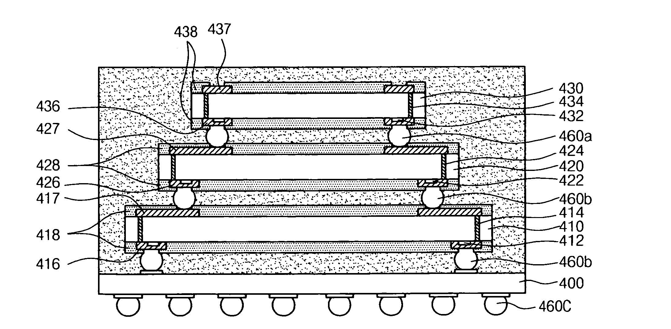
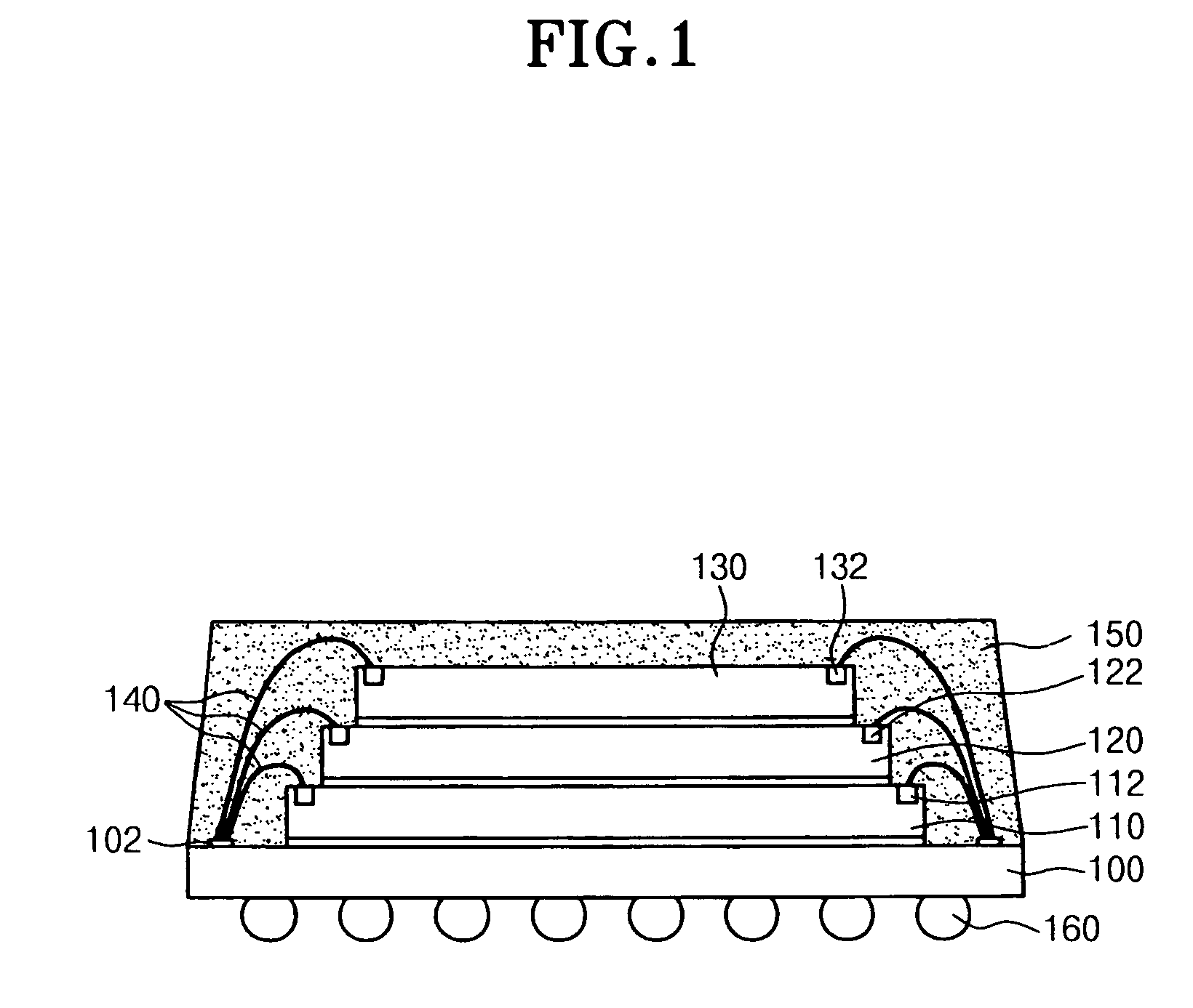
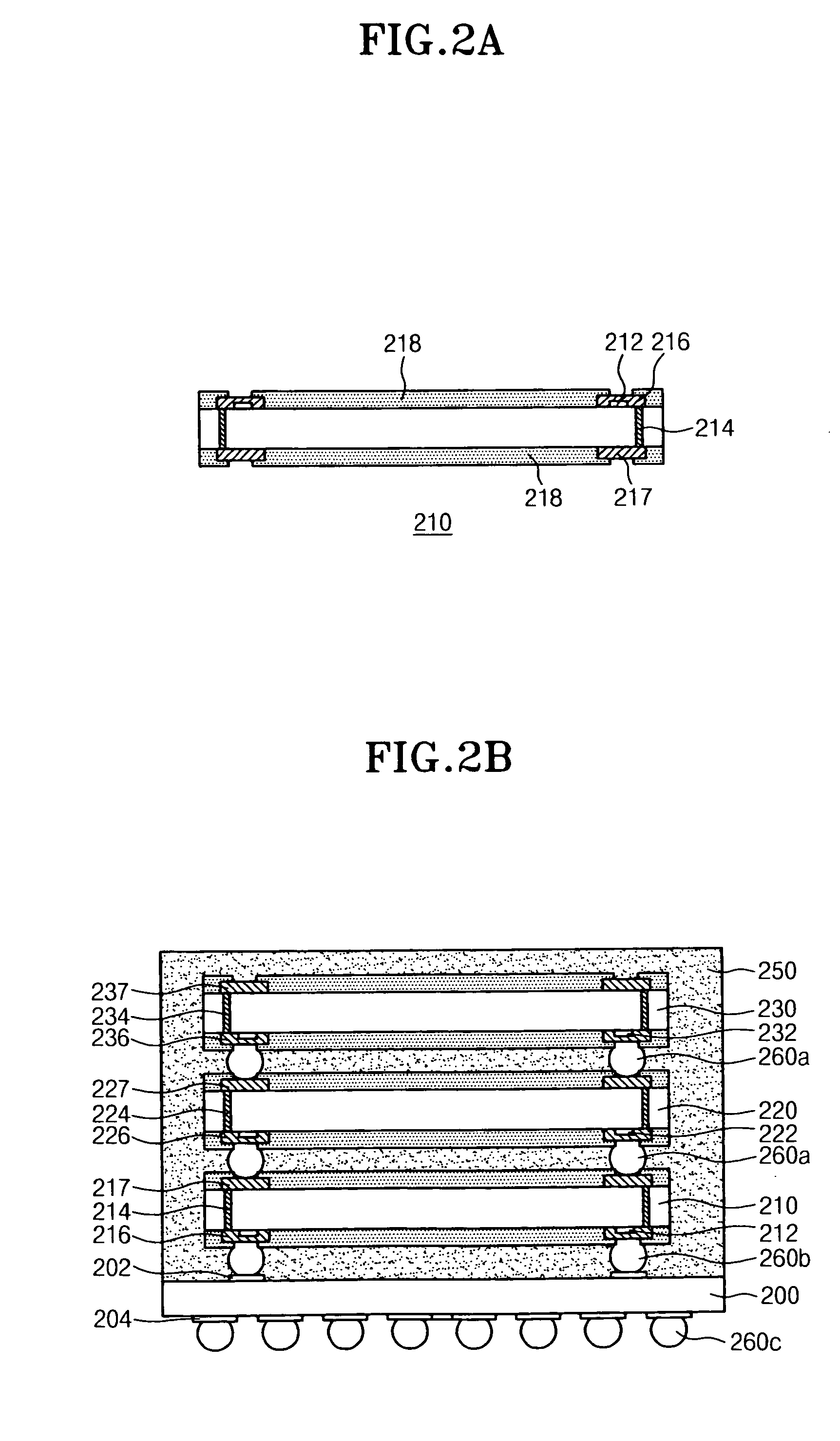
[0023]In the present invention, through silicon vias (hereinafter referred to as “TSVs”) and re-distribution lines are formed in respective semiconductor chips to be stacked, and the stack of the aforementioned semiconductor chips is formed by connecting the re-distribution lines to one another.

[0024]In the stack package according to the present invention, the TSVs, re-distribution lines and solder balls form the electrical connections between the semiconductor chips, which provide several advantages. First, this allows the stack package to be applied to high-speed products through minimization of the electrical signal transmittance path. Second, not only semiconductor chips of different sizes but also semiconductor chips of the same size can be easily stacked upon one another without interposing a tape containing a shock-absorbing substance between two adjoining semiconductor chips. Third, the overall size of the stack package can be decreased since it is not necessary to consider ...


PUM


Abstract

A stack package includes a printed circuit board; at least two semiconductor chips stacked on the printed circuit board, each having first re-distribution lines formed on the upper surface thereof and connected to bonding pads, through silicon vias which are formed therethrough and connected to the first re-distribution lines, and second re-distribution lines formed on the lower surface thereof and connected to the through silicon vias; first and second solder balls interposed between the first and second re-distribution lines which face each other and between the first re-distribution lines of the lowermost semiconductor chip and electrode terminals of the printed circuit board; a molding material for molding the upper surface of the printed circuit board including the stacked semiconductor chips; and third solder balls attached to ball lands formed on the lower surface of the printed circuit board.

Description

CROSS-REFERENCE TO RELATED APPLICATIONS[0001]The present application claims priority to Korean patent application number 10-2006-0025054 filed on Mar. 17, 2006, which is incorporated by reference in its entirety.BACKGROUND OF THE INVENTION[0002]The present invention relates to a stack package, and more particularly, to a stack package using re-distribution lines and solder balls.[0003]As the performances of electric and electronic products are improved, techniques for mounting an increased number of packages to a substrate having a limited size have been researched. Generally, in a stack package, one semiconductor chip is mounted to a substrate, which increases the difficulty of attaining a desired capacity.[0004]As a method of increasing the capacity of a memory chip, that is, for accomplishing high integration, it is generally known in the art that an increased number of cells are formed in a limited space. However, this method requires use of high-precision process techniques inv...

Claims


Application Information

Patent Timeline
IPC IPC(8): H01L23/02
CPCH01L23/481H01L25/0657H01L24/48H01L2924/15311H01L2924/01079H01L2225/06541H01L2225/06527H01L2225/06517H01L2225/06513H01L2224/73265H01L2224/48227H01L2224/48091H01L2224/32225H01L2224/32145H01L2224/16145H01L2224/16225H01L2924/00014H01L2924/00H01L24/02H01L24/05H01L24/13H01L24/45H01L2224/02372H01L2224/02377H01L2224/05001H01L2224/05008H01L2224/05009H01L2224/05024H01L2224/05144H01L2224/05147H01L2224/05155H01L2224/05548H01L2224/05647H01L2224/0615H01L2224/06181H01L2224/13024H01L2224/17181H01L2224/451H01L2924/0001H01L2924/181H01L2924/00015H01L2224/05599H01L2924/00012H01L2224/02B42D1/005B42D5/002B44D5/10
Inventor LEE, SEUNG HYUNSUH, MIN SUK
Owner SK HYNIX INC
Why Eureka
Try Eureka