

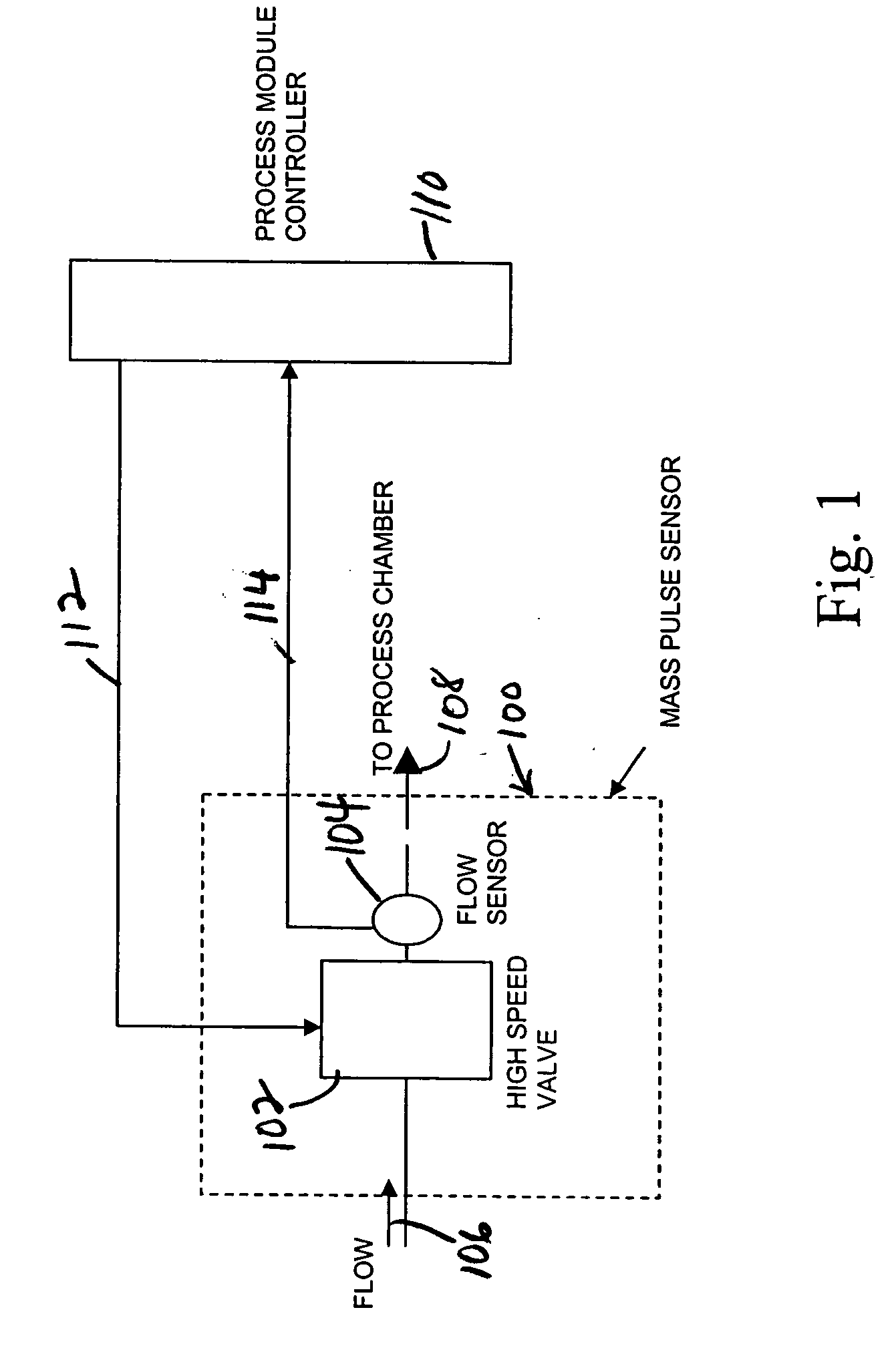
Mass pulse sensor and process-gas system and method
a mass pulse sensor and process gas technology, which is applied in the direction of valve arrangements, engine components, electrical apparatus, etc., can solve the problems of increasing the density and complexity of the device, accumulating errors in the device being manufactured, and traditional gas delivery, control and measurement technologies that exhibit response times of approximately 1 second
- Summary
- Abstract
- Description
- Claims
- Application Information
AI Technical Summary
Benefits of technology
Problems solved by technology
Method used
Image

Examples
Embodiment Construction
[0018] The stringent requirements of the most advanced devices as well as projected future device devices have led to the development of advanced deposition techniques such as atomic layer deposition (ALD), sequential layer deposition, cyclic layer deposition, nano layer deposition (NLD), and the like. The “time scale” of the reactions used in these advanced deposition techniques is generally on the order of less than 1 second for each step. Traditional gas delivery, control, and measurement technologies that exhibit response times of approximately 1 second are not suitable for these technologies.
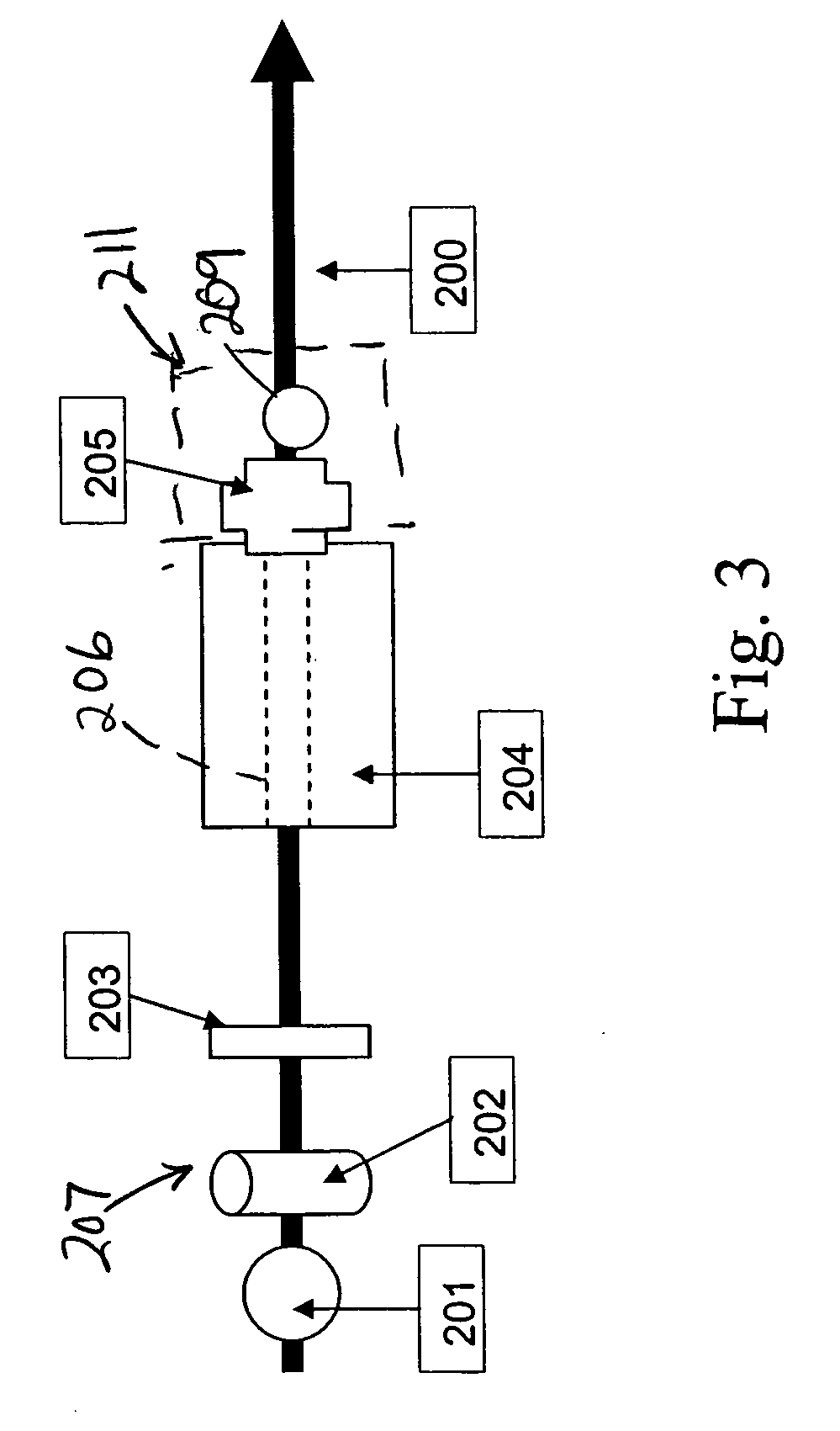
[0019] In the ALD process method, a substrate is exposed to a first precursor. Ideally, the precursor saturates the surface and forms a single monolayer on substrate. Excess amounts of the precursor do not react and are carried away through the system exhaust system. The process chamber is purged to remove the unreacted precursor and a second reactive gas is introduced. The second reactive...
PUM
 Abstract
Description
Claims
Application Information