Facility with Multi-Storied Process Chamber for Cleaning Substrates and Method for Cleaning Substrates Using the Facility

Active Publication Date: 2007-09-27
SEMES CO LTD
View PDF6 Cites 22 Cited by
  • Summary
  • Abstract
  • Description
  • Claims
  • Application Information

AI Technical Summary

Benefits of technology

[0007] Exemplary embodiments of the present invention provides a cleaning facility for efficiently p

Problems solved by technology

Unfortunately, the foregoing cleaning facility occupies a very large area because of a number of processing baths, a loading part, and an unl

Method used


Image

  • Facility with Multi-Storied Process Chamber for Cleaning Substrates and Method for Cleaning Substrates Using the Facility
  • Facility with Multi-Storied Process Chamber for Cleaning Substrates and Method for Cleaning Substrates Using the Facility
  • Facility with Multi-Storied Process Chamber for Cleaning Substrates and Method for Cleaning Substrates Using the Facility

Examples


Example

[0038] The present invention will now be described more fully hereinafter with reference to the accompanying drawings, in which preferred embodiments of the invention are shown. The invention may, however, be embodied in different forms and should not be construed as limited to the embodiments set forth herein. Rather, these embodiments are provided so that this disclosure will be thorough and complete, and will fully convey the scope of the invention to those skilled in the art. Like numbers refer to like elements throughout.

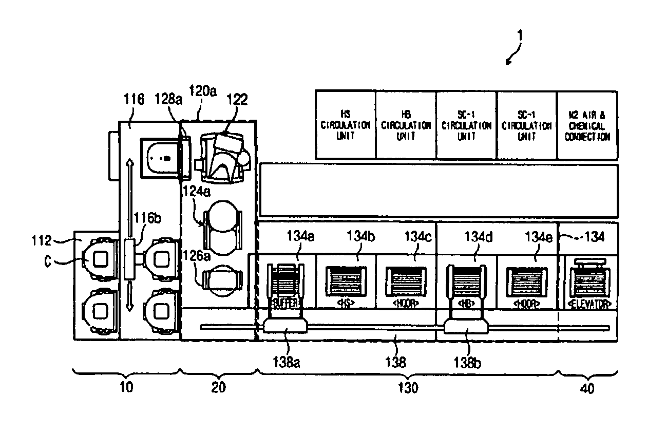
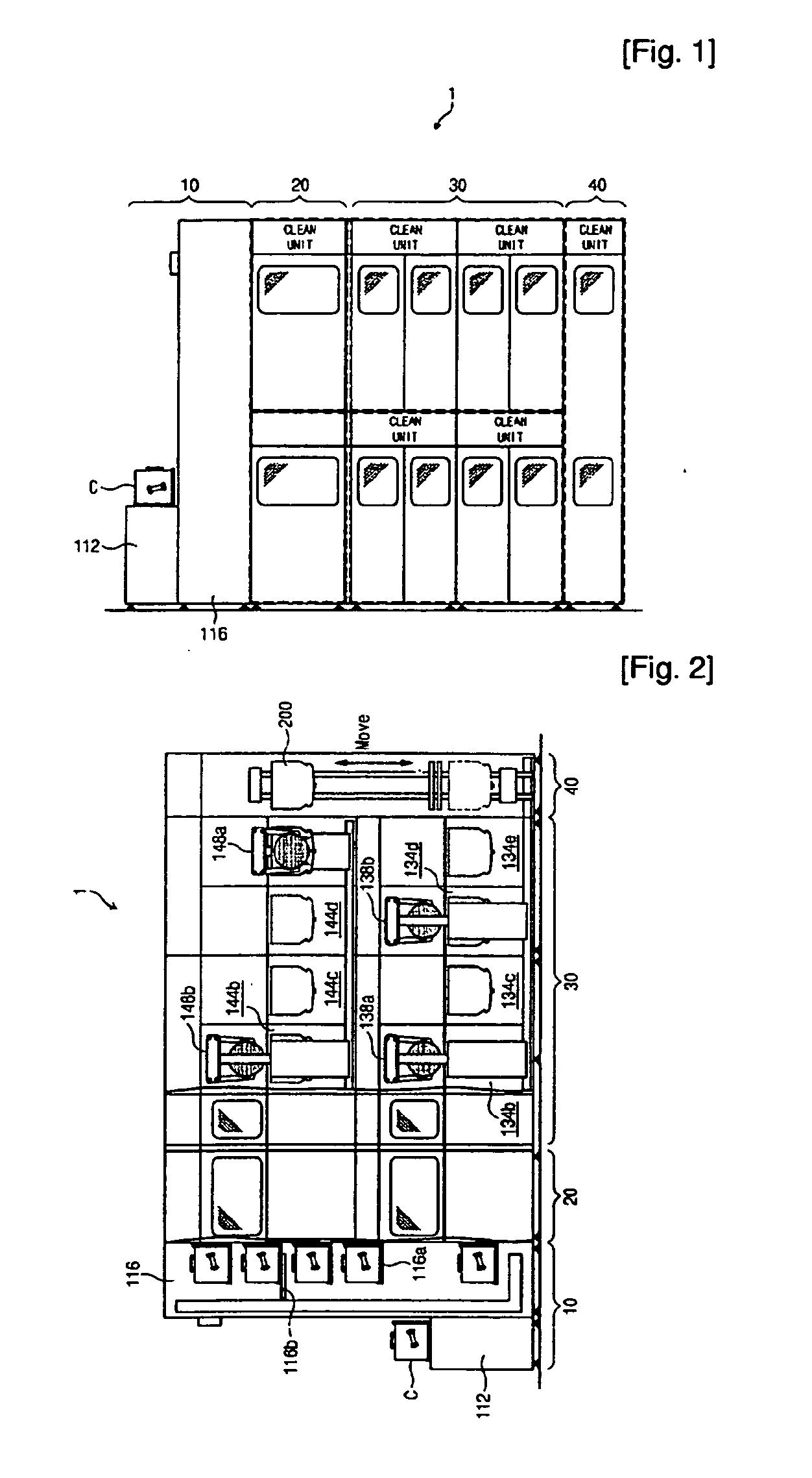
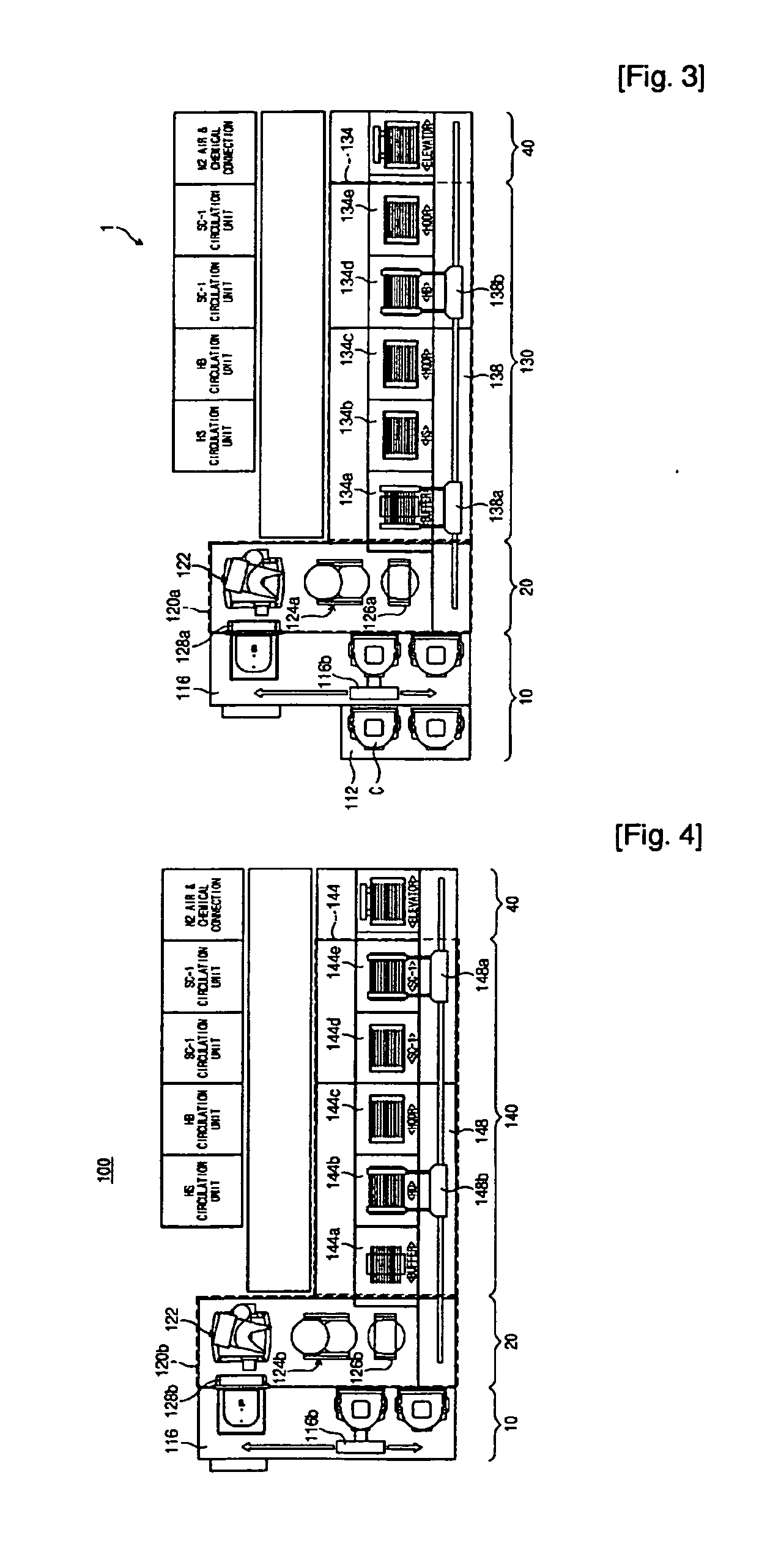
[0039] A configuration of a cleaning facility 1 according to the present invention is illustrated in FIG. 1. The cleaning facility 1 includes a loading / unloading part 10, an aligning part 20, a cleaning part 30, and an interface part 40 which may be disposed in a row. A cassette “C” containing to-be-processed wafers and a cassette “C” containing processed wafers are placed on the loading / unloading part 10. Wafers drawn out from the loading / unloading part 10 or...


PUM


Abstract

A facility for cleaning substrates such as semiconductor wafers includes a loading/unloading part, an aligning part where wafers are repositioned from a horizontal state to a vertical state, a cleaning part performing etchant-treating, rinsing, and drying processes for wafers and having a plurality of process chamber stacked, and an interface part where a transfer bath is disposed to transfer wafers between the process chambers. When the wafers are transferred between the process chamber, the transfer bath is filled with deionized water (DI water) to prevent their exposure to the air. Wafers drawn out of the loading/unlading part are repositioned from a horizontal state to a vertical state and are transferred to a first process chamber being one of the process chambers to be subjected to a part of processes. After the wafers are transferred to a second process chamber being the other one of the process chambers to be subjected to the other processes, they are repositioned from a vertical state to a horizontal state. That is, the wafers are transferred along a loop shape to be processed.

Description

BRIEF DESCRIPTION OF THE DRAWINGS [0001] 1. Technical Field [0002] The present invention relates to facility and method for manufacturing semiconductor devices and, more particularly, to facility and method for cleaning substrates such as semiconductor wafers. [0003] 2. Background Art [0004] When a semiconductor wafer is manufactured with integrated circuits, a wafer cleaning process must be performed to remove residual chemicals, small particles, contaminants or the like. The wafer cleaning process comprises an chemical treating process for etching or removing contaminants on a wafer using a chemical reaction, a rinsing process for rinsing an chemically treated wafer using deionized water (DI water), and a drying process for finally drying a wafer. In order to perform these processes, a variety of processing baths are used. The processing baths includes, for example, a processing bath in which a mixed solution of ammonium hydroxide (NH4OH), hydrogen peroxide (H2O2), and water (H2O)...

Claims


Application Information

Patent Timeline
IPC IPC(8): H01L21/302H01L21/00H01L21/304H01L21/677
CPCH01L21/67017H01L21/67028H01L21/67051H01L21/67745H01L21/67173H01L21/67207H01L21/67057
Inventor LIM, JOUNG-HYEONCHO, JUNG-KEUNKOO, KYO-WOOGBANG, IN-HOKIM, WOO-YOUNGOH, MAN-SEOKKIM, HYUN-JONG
Owner SEMES CO LTD
Why Eureka
Try Eureka