Pixel driving method and flat panel display thereof
a driving method and flat panel technology, applied in the direction of instruments, static indicating devices, etc., can solve the problems of increasing the resolution, increasing the cost of the driving circuit and the cost of the flat panel display, and increasing the charging capacity of the pixel
- Summary
- Abstract
- Description
- Claims
- Application Information
AI Technical Summary
Benefits of technology
Problems solved by technology
Method used
Image


Examples
Embodiment Construction
[0021]Referring to FIG. 3, a flat panel display according to a preferable embodiment of the invention is shown. A flat panel display 300, for example, is a liquid crystal display (LCD) comprising a substrate 312, a scan line driving circuit 320 and a data line driving circuit 330. Sited on the substrate 312 are a number of scan lines G, a number of data lines D and a display area 310. The display area 310 is operable to display a frame and has a number of pixel rows (not shown). The scan line driving circuit 320 and the data line driving circuit 330 are separately connected to the display area 310 through the scan lines G and the data lines D. In a normal driving mode, the scan line driving circuit 320 outputs scan voltages through the scan lines G to the substrate 312 to enable the corresponding pixels. The data line driving circuit 330 outputs data voltages through the data lines in order to display the pixels.
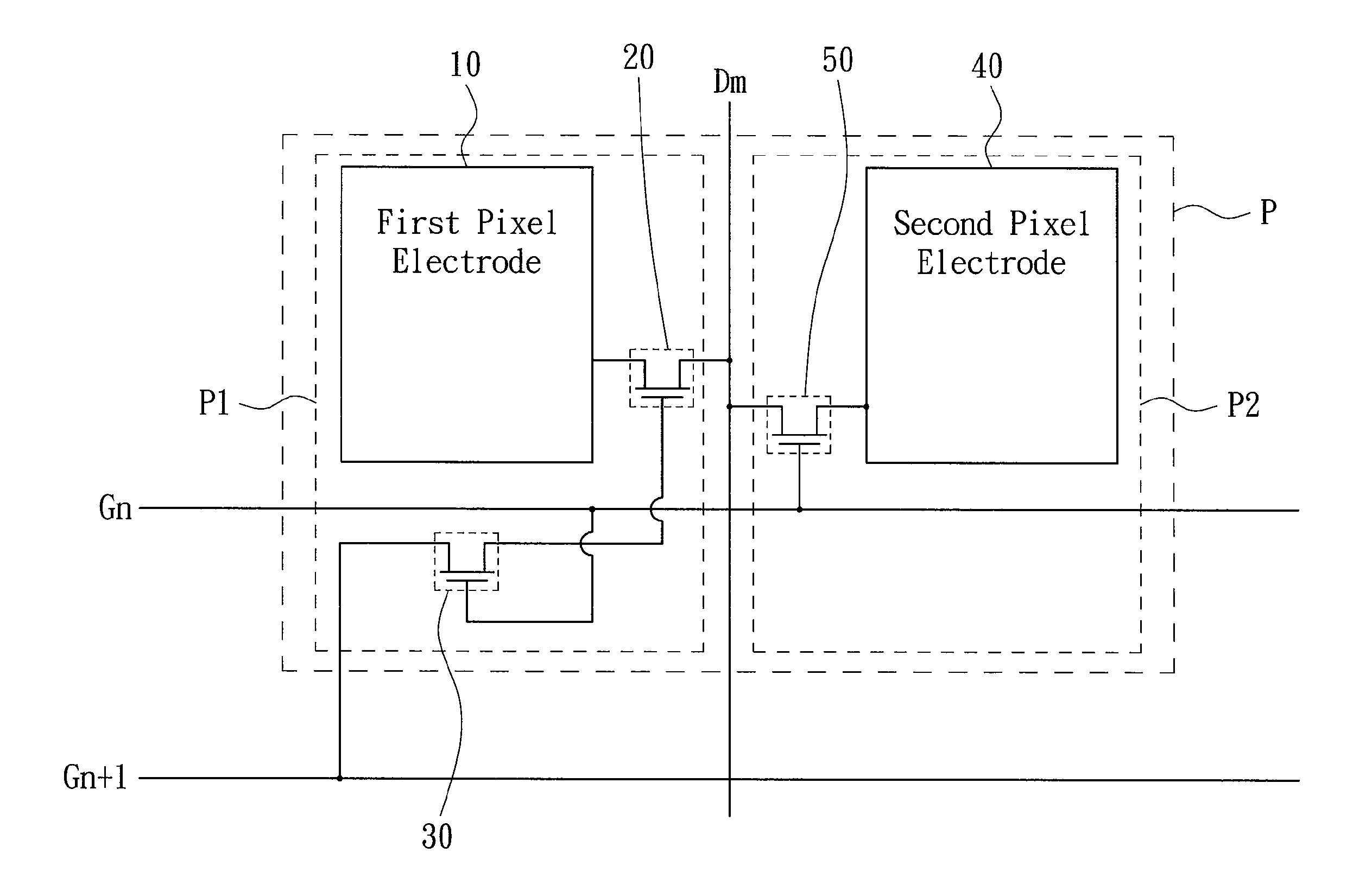
[0022]Referring to FIG. 4, a circuit structure of a pixel in the displa...
PUM
 Abstract
Description
Claims
Application Information