
Integrated circuit having multiple power domains

a technology of integrated circuits and power domains, applied in the field of integrated circuits, can solve the problems of increasing the number of power lines, increasing the ir voltage drop, and requiring more complicated integrated circuits

Active Publication Date: 2007-10-04
SAMSUNG ELECTRONICS CO LTD
View PDF7 Cites 40 Cited by
  • Summary
  • Abstract
  • Description
  • Claims
  • Application Information

AI Technical Summary

Benefits of technology

[0017]In this manner, the first and second power domains are separated for minimizing power consumption when the integrated circuit does not operate in the predetermined operating mode. However, the first and second power domains are connected for more flexible control of current flow therein during the predetermined operating mode when high frequency operation is more critical.

Problems solved by technology

Thus, the resistance of the power line increases that in turn significantly increases the IR voltage drop.
In addition, more complicated integrated circuits are fabricated with more gates for high performance.
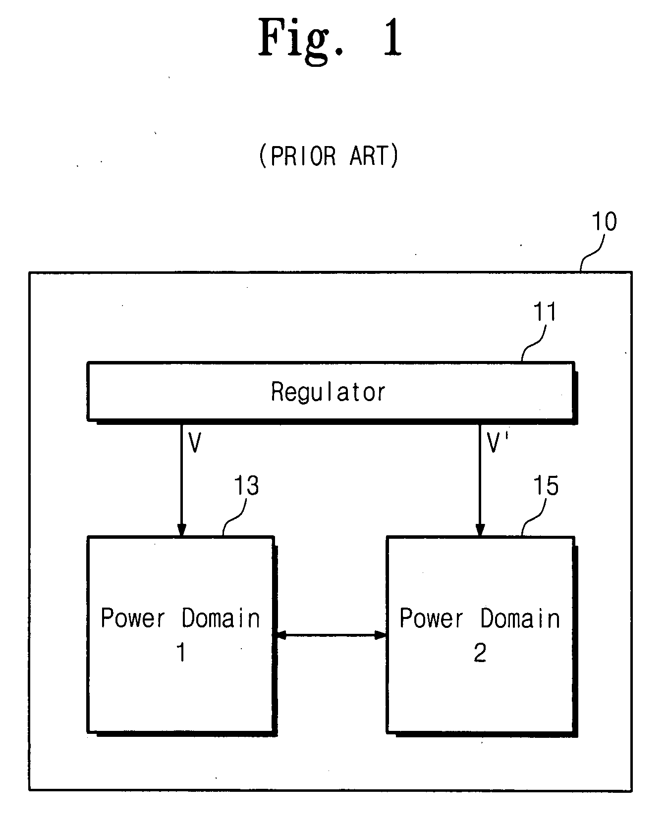
Thus in the prior art, the IR voltage drops in the separated power domains 13 and 15 may be higher and more difficult to control than when the integrated circuit has one power domain.

Method used


Image

  • Integrated circuit having multiple power domains
  • Integrated circuit having multiple power domains
  • Integrated circuit having multiple power domains

Examples


Embodiment Construction

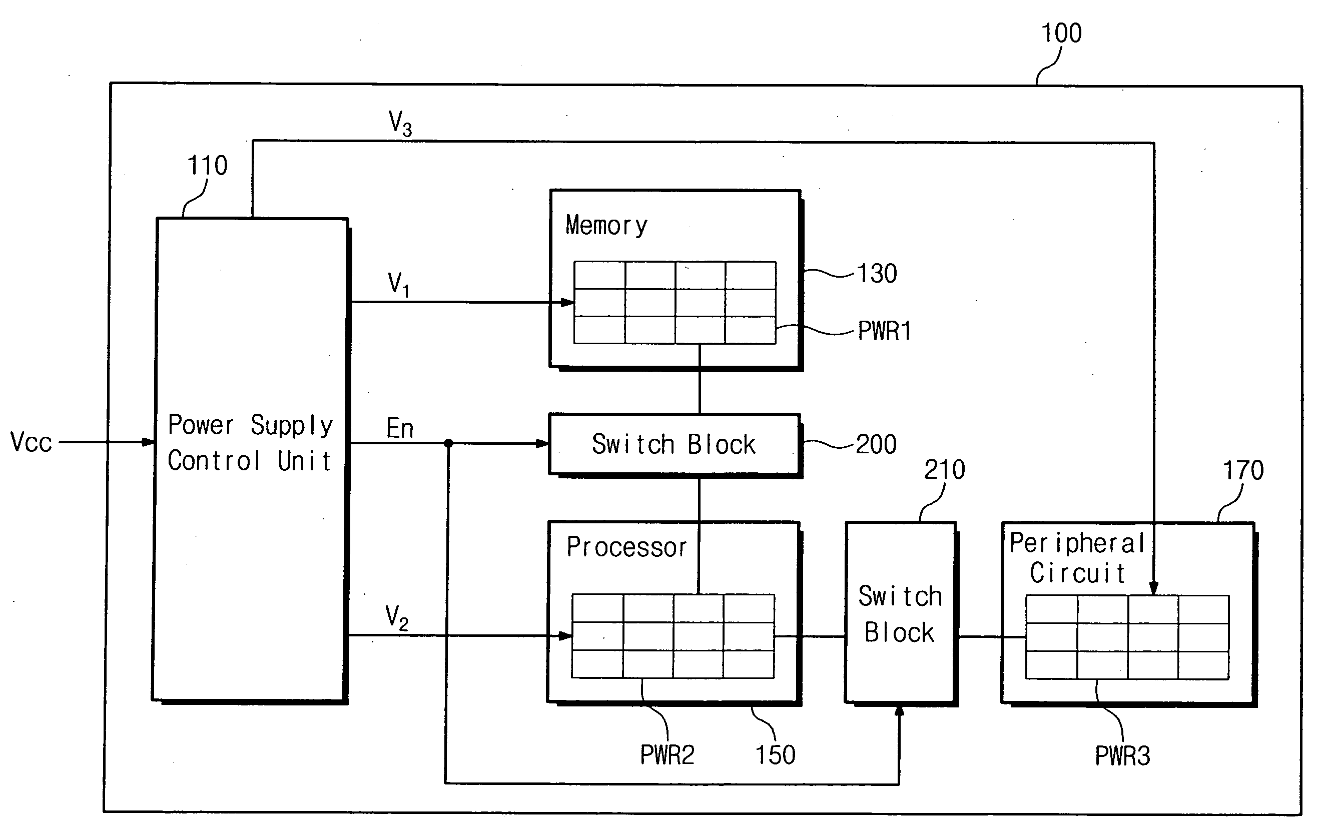
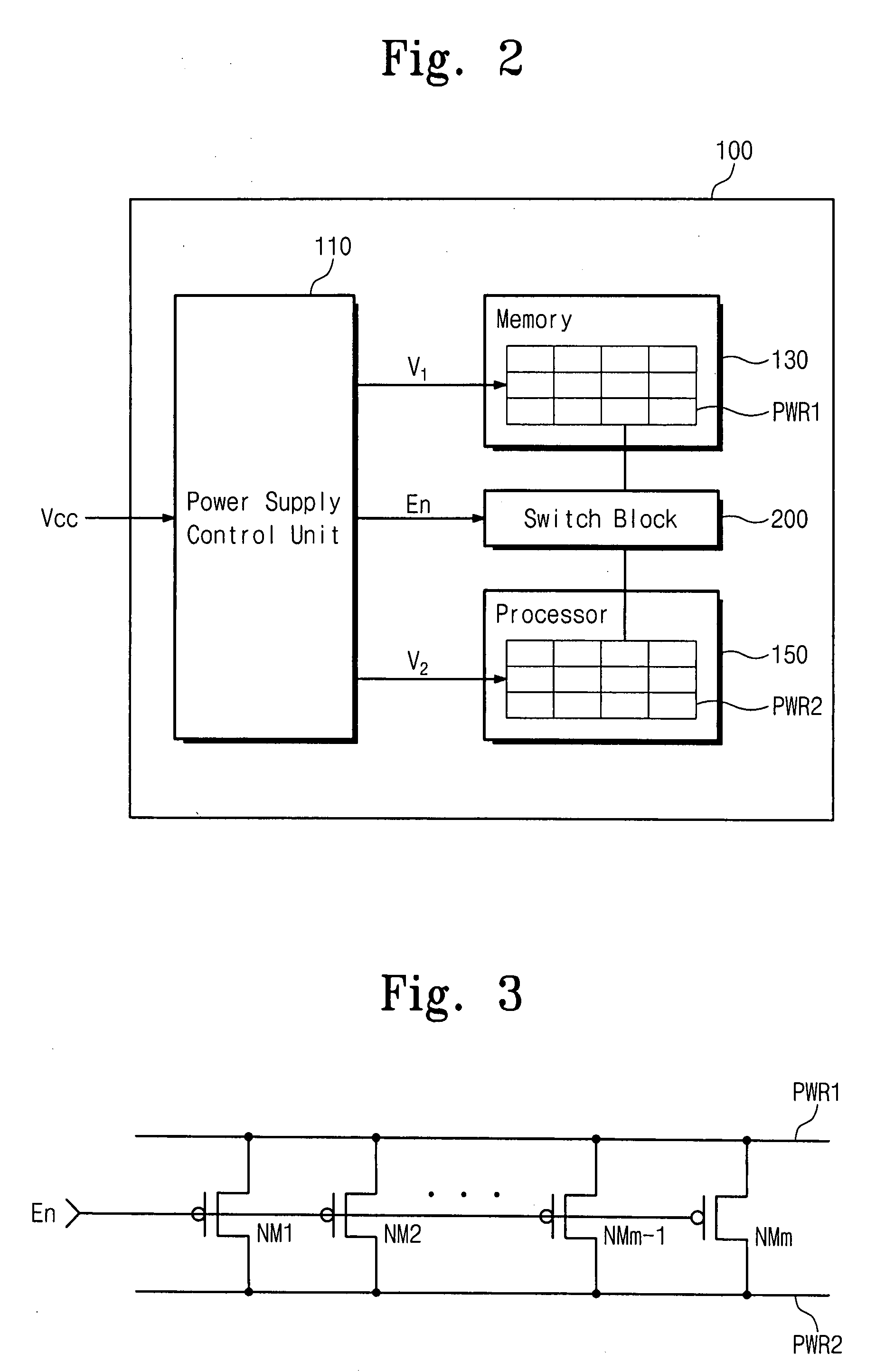
[0024]FIG. 2 is a block diagram of a semiconductor integrated circuit 100 according to an embodiment of the present invention. Referring to FIG. 2, the integrated circuit 100 includes a power supply control unit 110, a memory unit 130, a processor 150, and a switch block 200. The memory unit 130 and the processor 150 are implemented as separate power domains that are physically separated. That is, the power domains 130 and 150 have separate physical power supply lines for receiving respective operating voltages applied thereon.

[0025]Referring to FIG. 2, the power supply control unit 110 provides respective operating voltages V1 and V2 to the multiple power domains 130 and 150. The power supply control unit 110 may be fabricated as part of the integrated circuit 100 or may be formed outside the integrated circuit 100. If formed outside the integrated circuit 100, the integrated circuit 100 has separate pins receiving the operating voltages V1 and V2 from the external power supply con...


PUM


Abstract

An integrated circuit includes first and second power domains, a power supply control unit, and a switch block. The power supply control unit supplies a first voltage to the first power domain and a second voltage to the second power domain. The switch block provides at least one current path between the first and second power domains during a predetermined operating mode such as by connecting a first power line of the first power domain to a second power line of the second power domain.

Description

BACKGROUND OF THE INVENTION[0001]This application claims priority under 35 USC §119 to Korean Patent Application No. 2006-19485, filed on Feb. 28, 2006 in the Korean Intellectual Property Office, the disclosure of which is incorporated herein in its entirety by reference.FIELD OF THE INVENTION[0002]The present invention relates generally to integrated circuits, and more particularly, to an integrated circuit having multiple power domains with power lines that are connected together in a predetermined operating mode.BACKGROUND OF THE INVENTION[0003]A semiconductor integrated circuit fabricated as a conventional flash memory has generally used a power voltage of 5 Volts as an operating voltage. However, lower operating voltages are desired with higher integration and scaling-down of semiconductor integration circuits. For example, an operating voltage of about 1.0 V is used for a memory device, and an operating voltage of from about 0.6 Volts to about 1.3 Volts is used for a logic cir...

Claims


Application Information

Patent Timeline
Patent Type & Authority Applications(United States)
IPC IPC(8): G06F1/00
CPCG06F1/3203G06F1/3243Y02B60/1285Y02B60/1239G06F1/3296Y02D10/00F25D11/02F25D25/028F25D17/067F25D2400/28
Inventor LEE, HOI-JIN
Owner SAMSUNG ELECTRONICS CO LTD
Learn More