Devices with microjetted polymer standoffs

a technology of standoffs and polymers, applied in the direction of final product manufacturing, semiconductor/solid-state device details, sustainable manufacturing/processing, etc., can solve the problems of only providing support, device collapse, and negative impact on the reliability of solder joints, so as to prevent the collapse of electronic devices

Inactive Publication Date: 2007-10-11
DELPHI TECH INC
View PDF18 Cites 74 Cited by
  • Summary
  • Abstract
  • Description
  • Claims
  • Application Information

AI Technical Summary

Benefits of technology

[0007] In one aspect, the invention provides an electronic package comprising a substrate having electrically conductive pathways and at least one conductive mounting pad, a surface mount electronic device having at least one terminal, and a plurality of polymeric standoffs adhered to at least one of the underside of the surface mount electronic device or an upper surface of the substrate to maintain a desired gap between the undersid...

Problems solved by technology

However, overmolding conventional surface mount components, such as flip chips or the like, can lead to device collapse due to the extreme pressure that is placed on the component during the molding ope...

Method used


Image

  • Devices with microjetted polymer standoffs
  • Devices with microjetted polymer standoffs

Examples


Embodiment Construction

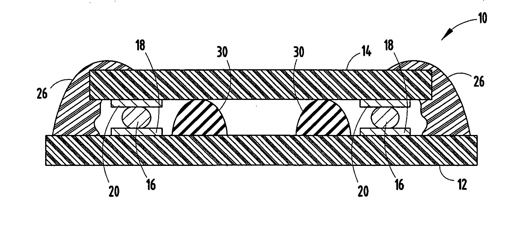
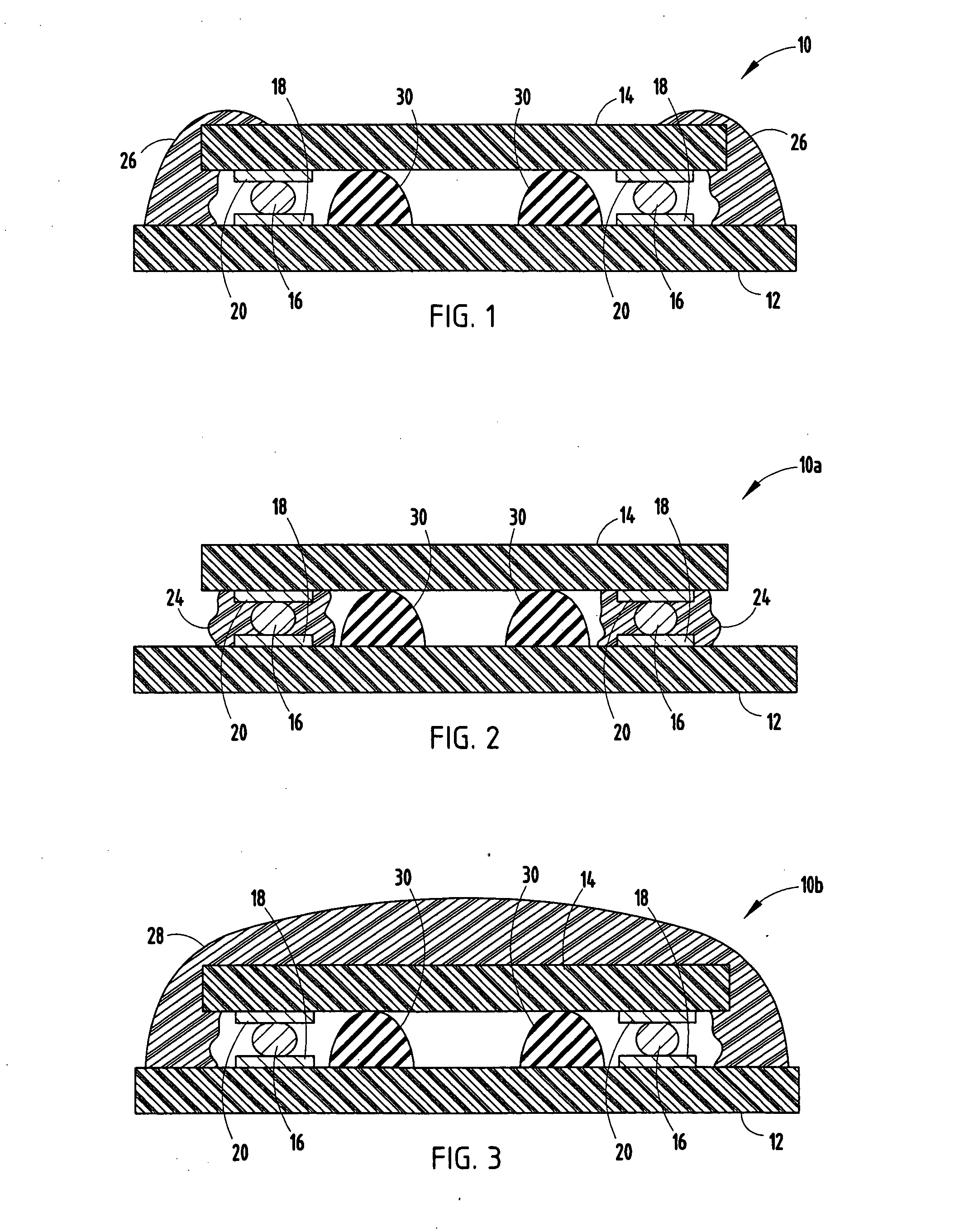
[0014] Referring to FIG. 1, an electronic package 10 comprises a substrate 12 having printed or otherwise disposed thereon electrically conductive pathways or traces that together with one or more electronic components mounted on the substrate define an electronic component package. A surface mount electronic device 14 is connected to the circuit board 12 by a solder joint 16. While the illustrated embodiment includes only a single surface mount electronic device 14, it should be appreciated that electronic package 10 may include any number of surface mount electronic devices 14 connected to substrate 12.

[0015] Substrate 12 may include a printed circuit board having a dielectric substrate and electrically conductive circuitry, such as printed circuit traces as should be evident to those skilled in the art. Substrate 12 may include electrical circuitry fabricated on both the upper and lower surfaces thereof, as well as electrical circuitry located in intermediate layers of the subst...


PUM


Abstract

An electronic package having a controlled standoff height between a surface mount electronic device and a substrate includes a plurality of polymeric standoffs adhered to at least one of the underside of the surface mount electronic device or an upper surface of the substrate. The polymeric standoffs prevent collapse of the surface mount electronic device during overmolding or encapsulation of the surface mount electronic device.

Description

TECHNICAL FIELD [0001] This invention pertains to electronic semiconductor packages and more particularly to electronic semiconductor packages having standoffs between a substrate and an electronic device mounted on the substrate. BACKGROUND OF THE INVENTION [0002] Electronic semiconductor packages are typically comprised of a substrate, such as a printed circuit board, and electronic components or chips that are mounted on the substrate and electrically connected to conductors on the substrate. In order to achieve smaller electronic semiconductor packages, so-called “surface mount” or lead-less electronic components are often preferred. These surface mount electronic components are characterized by the absence of electrical lead wires. Instead, electrical connections between the surface component and the substrate are achieved by a soldered joint located between a terminal on the component and a mounting pad on the substrate and in direct contact with the terminal and mounting pad....

Claims


Application Information

Patent Timeline
IPC IPC(8): H05K1/16
CPCH01L21/563H01L2224/11334H01L2224/16225H01L2224/73203H01L2224/81136H01L2224/8121H01L2224/81815H01L2224/83102H01L2224/83192H01L2224/83194H01L2224/92125H01L2924/01005H01L2924/01013H01L2924/01027H01L2924/01029H01L2924/0105H01L2924/01074H01L2924/01082H01L2924/01322H01L2924/09701H01L2924/19041H01L2924/19042H01L2924/19043H05K3/303H05K3/3436H05K2201/09909H05K2201/10674H05K2201/10977H05K2201/2036H05K2203/013H01L24/29H01L2924/01006H01L2224/10165H01L2224/8114H01L23/315H01L2224/05568H01L2224/05573H01L2924/00014H01L2924/12042H01L2924/15787Y02P70/50H01L2924/00H01L2224/05599
Inventor WORKMAN, DEREK B.
Owner DELPHI TECH INC
Why Eureka
Try Eureka